
Insulation frame structure for press-contact IGBT

An insulating frame and crimping type technology, which is applied in the direction of electrical components, electric solid devices, circuits, etc., can solve problems such as difficult to meet creepage distance, general type and weak stability, crimping chip dislocation, etc., to achieve universality And the effect of strong stability, excellent mechanical properties and simple positioning

Pending Publication Date: 2019-11-05
GLOBAL ENERGY INTERCONNECTION RES INST CO LTD
View PDF0 Cites 2 Cited by
  • Summary
  • Abstract
  • Description
  • Claims
  • Application Information

AI Technical Summary

Problems solved by technology

When the voltage level increases, the electrical clearance and creepage distance increase according to the regulations. In order to make the designed device highly versatile, the height should be as small as possible while meeting the electrical clearance. At this time, the annular shed structure is adopted. Difficult to meet creepage distance requirements
In addition, when the number of high-voltage IGBT parallel-connected chips increases, the crimped chips are prone to misalignment and lead to short-circuit failure. The existing technology uses an insulating frame structure with a ring shed that is bulky, general-purpose and weak in stability, difficult to process, and complex in positioning. Insulation coordination problems at high voltage levels

Method used


Image

  • Insulation frame structure for press-contact IGBT
  • Insulation frame structure for press-contact IGBT
  • Insulation frame structure for press-contact IGBT

Examples


Embodiment Construction

[0047] The present invention will be further described in detail below in conjunction with the drawings.

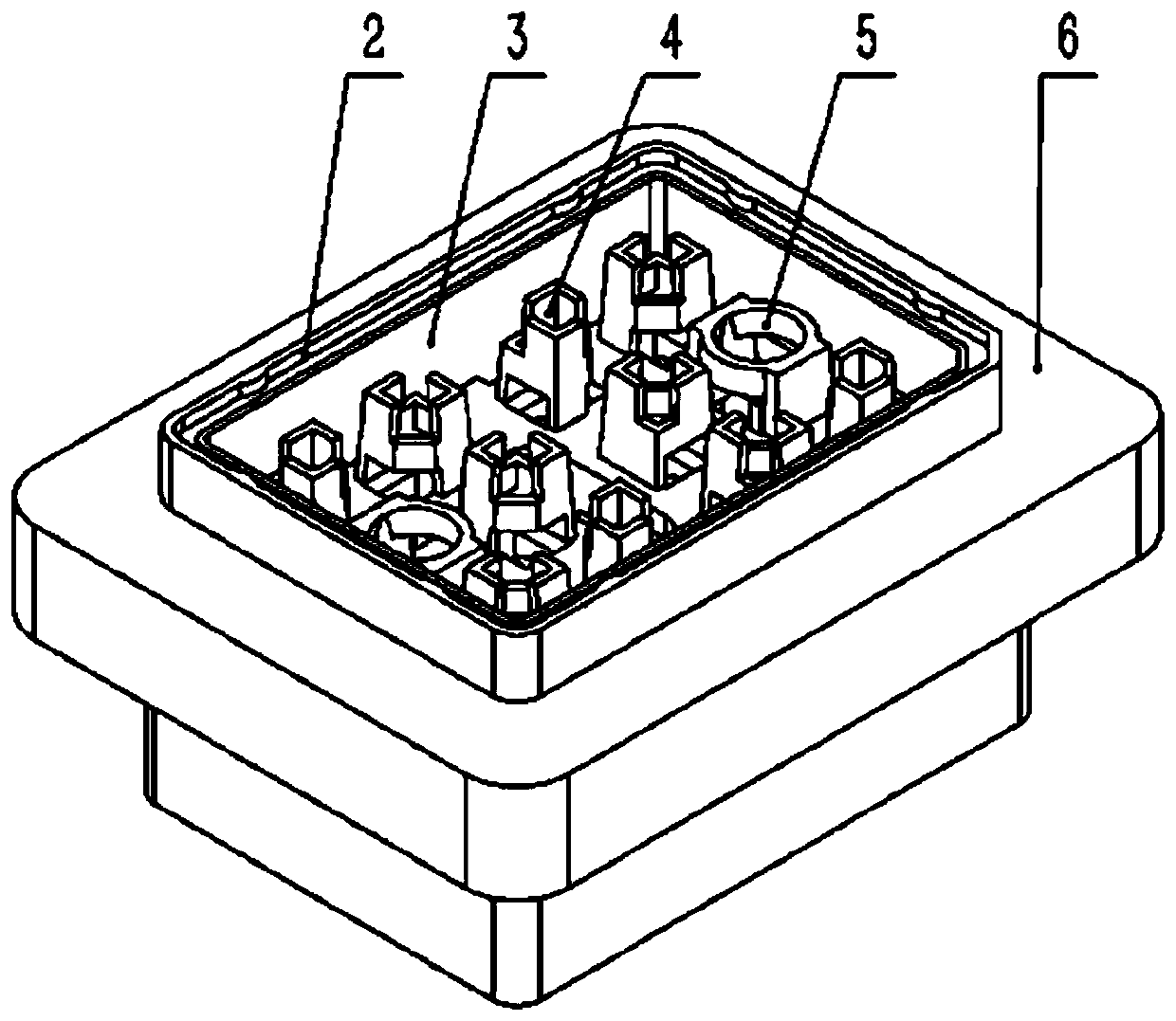
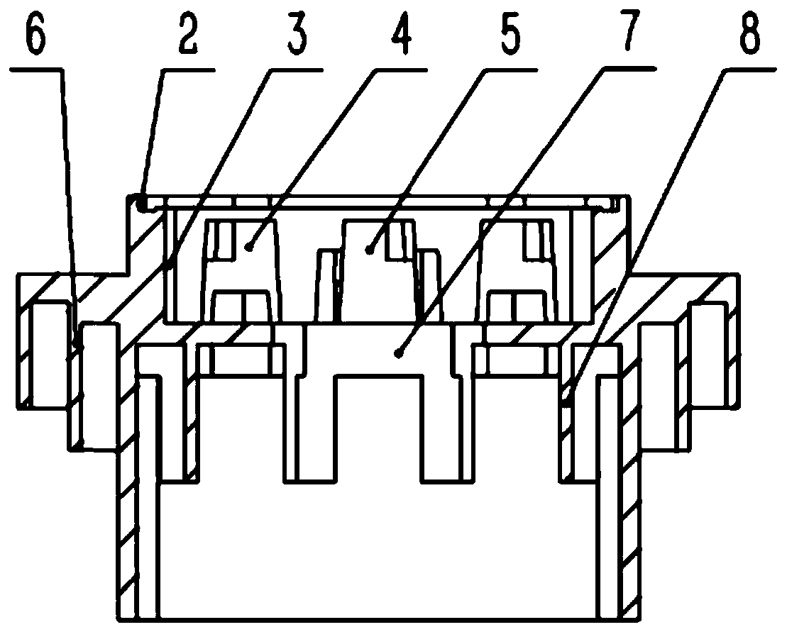
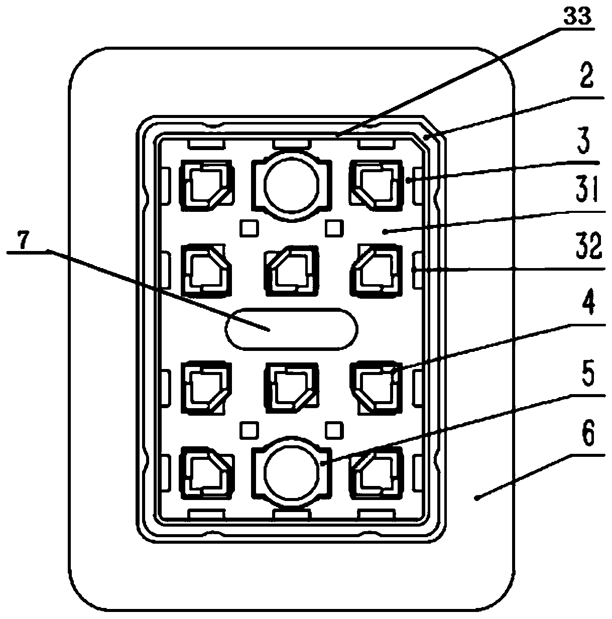
[0048] The embodiment of the present invention provides an insulating frame structure for crimping type IGBT, such as Figure 1-3 As shown, the insulating frame structure 1 includes an inner groove 3, an E pole post 4, a G pole post 5, a guide partition 8 and an umbrella skirt 6;

[0049] The guide partition 8 and the umbrella skirt 6 are respectively located on the lower side and the outer side of the inner groove 3, and the E pole column 4 and the G pole column 5 are both vertically arranged inside the inner groove 3;

[0050] The umbrella skirt 6 includes at least two layers of L-shaped umbrella skirt pieces arranged in sequence.

[0051] The number of umbrella skirt pieces increases successively with the increase of the voltage level. The embodiment of the present invention is provided with three layers of L-shaped umbrella skirt pieces, and the length of the L-shaped umbrell...


PUM


Abstract

The invention provides an insulation frame structure for a press-contact IGBT. The insulation frame structure comprises an inner groove, an E electrode upright column, a G electrode upright column, aguiding partition and a shed. The guiding partition and the shed are respectively located on the downside and the outside of the inner groove. The E electrode upright column and the G electrode upright column are vertically disposed inside the inner groove. The shed includes at least two layers of L-shaped shed sheets arranged in sequence. The insulation frame structure provided by the invention has small size, and high versatility and stability, is easy to process and simple for positioning, can effectively solve the problem of insulation coordination under different high voltage levels, andmeets fixed positioning requirements of a multi-chip parallel structure inside a device. The insulation frame structure made by open-die injection moulding of modified plastics is processable in batchand has high electrical insulation strength, anti-creepage performance and excellent mechanical performance. A glue filling port and an exhaust hole are favorable for injecting silicon gel and removing air, thereby reducing partial discharge caused by bubbles and adverse effect caused by thermal expansion.

Description

Technical field [0001] The present invention relates to the technical field of power semiconductors, in particular to an insulating frame structure for a crimping type IGBT. Background technique [0002] Insulated Gate Bipolar Transistor (IGBT) has the advantages of easy drive control, high switching frequency, low turn-on voltage, and large on-state current. It is widely used as the key core component of automatic control and power conversion. It is used in converter systems with a DC voltage of 600V and above, such as rail transit, smart grid, aerospace, electric vehicles and new energy equipment. With the continuous progress of IGBT chip design and process technology, continuous innovation of module packaging concepts and materials, and strong market demand, IGBT devices are moving towards higher power density, higher operating frequency, higher operating temperature and higher reliability. Development, especially in the field of flexible DC transmission, high-voltage high-po...

Claims


Application Information

Patent Timeline
IPC IPC(8): H01L25/07H01L29/739H01L23/04H01L23/08
CPCH01L23/04H01L23/08H01L25/07H01L29/7393
Inventor 张雷杨晓亮杜玉杰李金元张西子陈艳芳
Owner GLOBAL ENERGY INTERCONNECTION RES INST CO LTD
Learn More