High-gain bandwidth product optical detector and manufacturing method thereof

A technology of photodetector and manufacturing method, applied in the direction of final product manufacturing, sustainable manufacturing/processing, semiconductor devices, etc., can solve problems such as low gain, and achieve the effect of high gain bandwidth product

Pending Publication Date: 2019-10-22
武汉光谷量子技术有限公司
View PDF0 Cites 2 Cited by
  • Summary
  • Abstract
  • Description
  • Claims
  • Application Information

AI Technical Summary

Problems solved by technology

WGAPD and ECAPD adopt a waveguide structure, so that light is incident from the side of the device, and a thinner active layer can be used without reducing the quantum efficiency to increase the bandwidth. The bandwidth of this type of APD can reach 35GHz, but the gain is low, and the gain bandwidth Product is about 140GHz

Method used


Image

  • High-gain bandwidth product optical detector and manufacturing method thereof
  • High-gain bandwidth product optical detector and manufacturing method thereof
  • High-gain bandwidth product optical detector and manufacturing method thereof

Examples


Embodiment Construction

[0029] The present invention will be described in further detail below in conjunction with the accompanying drawings and embodiments.

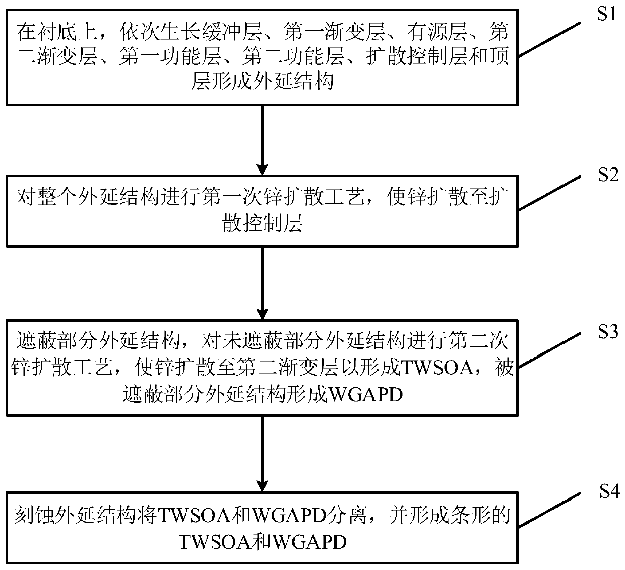
[0030] see figure 1 As shown, an embodiment of the present invention provides a method for manufacturing a photodetector with a high gain-bandwidth product, comprising the following steps:

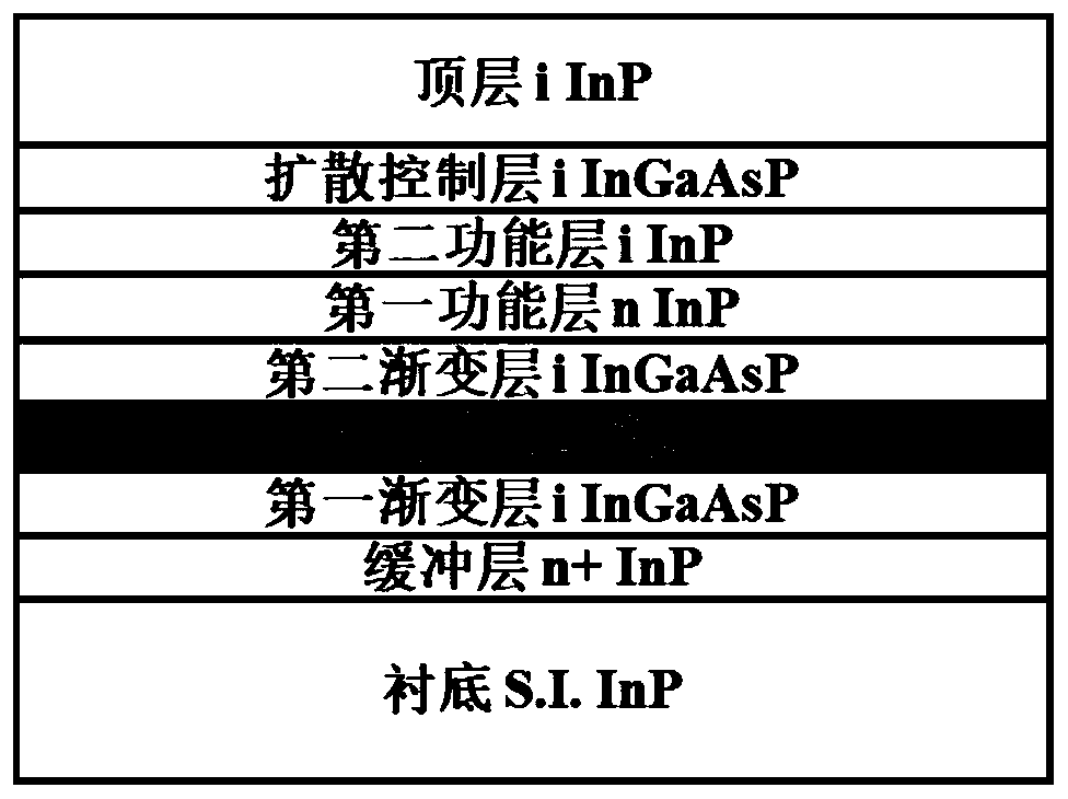
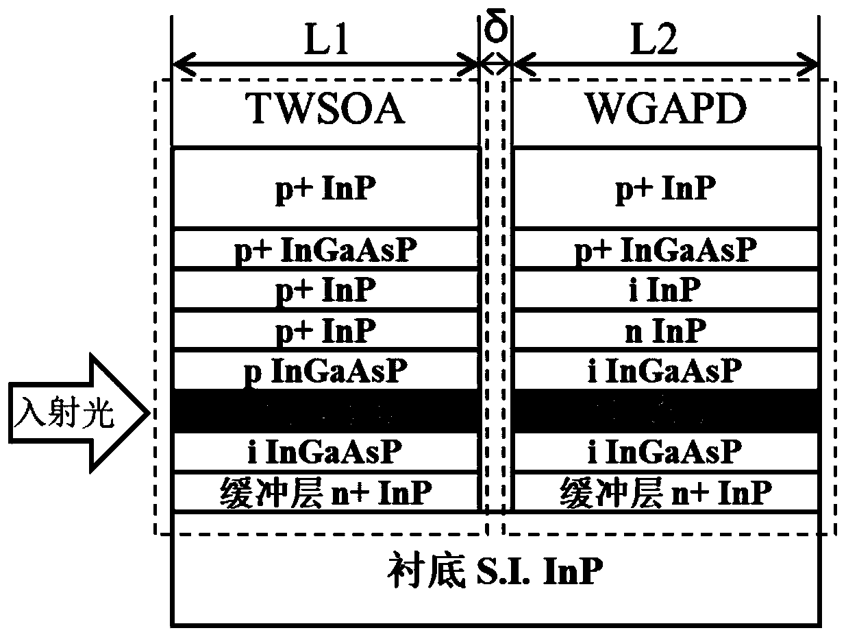
[0031] Step S1, on the substrate, sequentially grow a buffer layer, a first graded layer, an active layer, a second graded layer, a first functional layer, a second functional layer, a diffusion control layer and a top layer to form an epitaxial structure.

[0032] Specifically, see figure 2 As shown, on a semi-insulating (S.I., semi-insulating) indium phosphide InP substrate, epitaxial growth such as MBE (Molecular Beam Epitaxy) or metal-organic compound chemical vapor deposition (MOCVD (Metal-organic Chemical Vapor Deposition)) technology, growing the buffer layer, the first graded layer, the active layer, the second graded layer, the first functional...


PUM


Abstract

The invention discloses a manufacturing method of a high-gain bandwidth product optical detector, and relates to the technical field of optical detectors. The optical detector comprises the followingsteps: S1, sequentially growing a buffer layer, a first gradient layer, an active layer, a second gradient layer, a first functional layer, a second functional layer, a diffusion control layer and a top layer on a substrate to form an epitaxial structure; S2, performing a first zinc diffusion process on the whole epitaxial structure to diffuse zinc to the diffusion control layer; S3, shielding part of the epitaxial structure, and performing a second zinc diffusion process on the unshielded part of the epitaxial structure so as to diffuse zinc to the second gradient layer to form TWSOA, whereinWGAPD is formed on the shielded part of the epitaxial structure; S4, etching the epitaxial structure to separate the TWSOA from the WGAPD, and forming a strip-shaped TWSOA and a strip-shaped WGAPD; and S5, respectively manufacturing electrodes of the TWSOA and the WGAPD. The invention also discloses the optical detector with high-gain bandwidth product. The gain bandwidth product of the optical detector provided by the invention can reach 1000GHz.

Description

technical field [0001] The invention relates to the technical field of photodetectors, in particular to a photodetector with high gain-bandwidth product and a manufacturing method thereof. Background technique [0002] With the rapid development of the Internet of Things and 5G, the bandwidth requirements of optical fiber communication systems continue to increase. At present, the optical detector used in the high-speed optical signal receiving module adopts a planar avalanche photodiode (APD, Avalanche Photo Diode), which has internal gain and can amplify the current signal. The APD with a rate of 10Gbps has been widely used. However, the design and manufacture of APDs with a rate above 25Gbps is relatively difficult, which has become a limiting factor in the transmission rate of optical communication systems. The bandwidth of APD is mainly limited by the transit time of photogenerated carriers and the avalanche establishment time. At present, the 10Gbps APD adopts the ve...

Claims


Application Information

Patent Timeline
Patent Type & Authority Applications(China)
IPC IPC(8): H01L31/18H01L31/0232H01L31/0304H01L31/0352H01L31/107
CPCH01L31/03046H01L31/035209H01L31/035281H01L31/1075H01L31/02327H01L31/1844Y02P70/50
Inventor 曾磊王肇中
Owner 武汉光谷量子技术有限公司
Why Eureka
Try Eureka