Solar cell and preparation method thereof
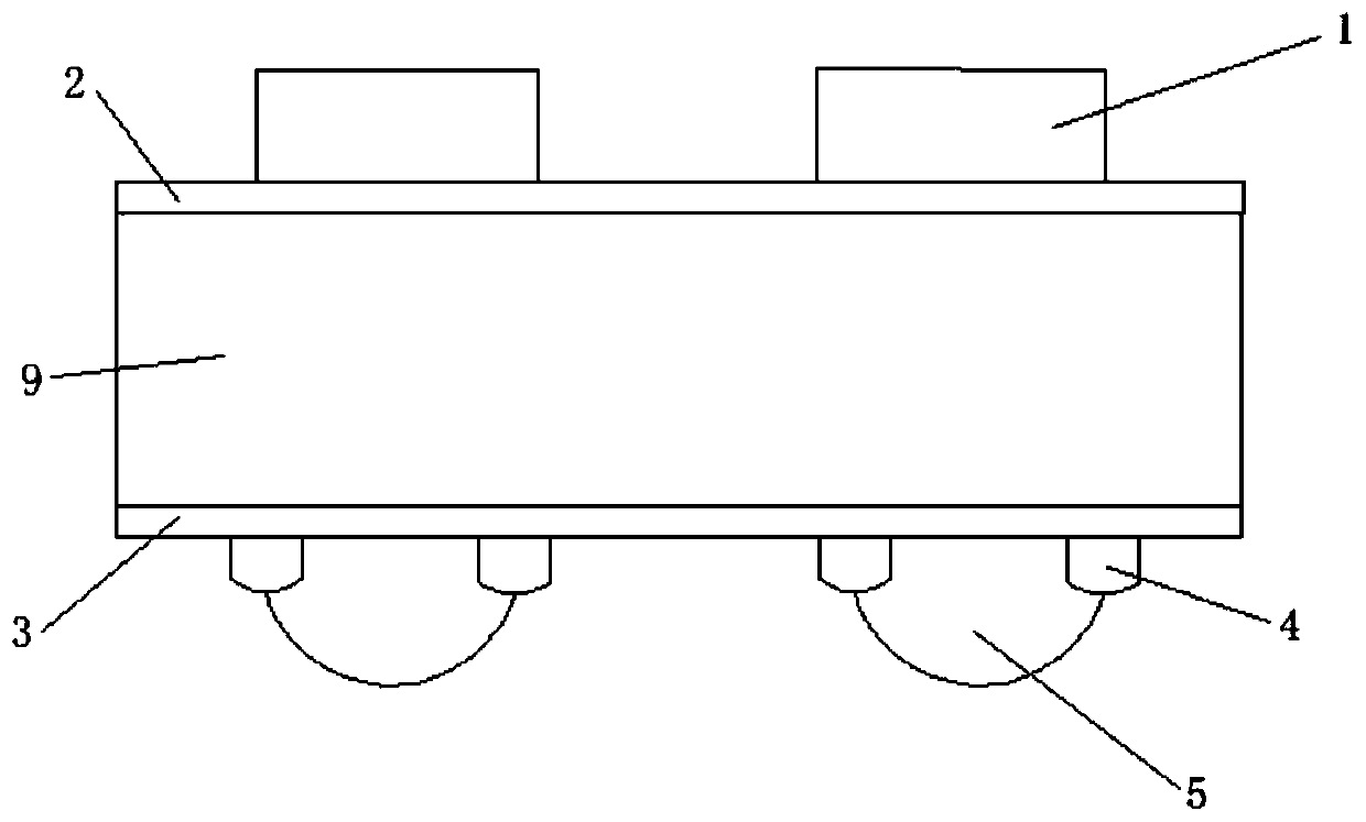
A solar cell and back electric field technology, applied in the field of solar cells, can solve the problems of low stability of the average conversion rate of PERC cells, large investment in upgrading PERC cell technology, and the efficiency of cells cannot meet market demand, etc., and achieve structural stability. , The effect of low production cost, good wear resistance and oxidation resistance
- Summary
- Abstract
- Description
- Claims
- Application Information
AI Technical Summary
Problems solved by technology
Method used
Image
Examples
Embodiment 1
[0022] Embodiment 1. A method for preparing a solar cell, specifically comprising the following steps:
[0023] 1. Carry out texturing on the front surface and the back surface of the silicon wafer.
[0024] 2. Use phosphorus oxychloride liquid source to carry out tubular phosphorus diffusion on the suede surface.
[0025] 3. Using HF, HNO 3 and other chemical solutions to etch the PN junction around the silicon wafer and on the back.
[0026] 4. Silicon nitride coating is performed on the front surface of the silicon wafer.
[0027] 5. Al on the back surface of the silicon body 2 o 3 Passivation, Al 2 o 3 Passivation film thickness is 10nm.
[0028] 6. After passivation, use silver paste to print the back electrode and dry it.
[0029] 7. Preparation of ceramic slurry: Ceramic slurry includes ceramic powder, dispersant, binder and solvent. The ceramic powder is 90 parts by weight, the dispersant is 2 parts by weight, the binder is 8 parts by weight, and the solvent i...
Embodiment 2
[0036] Embodiment 2. A method for preparing a solar cell, specifically comprising the following steps:
[0037] 1. Carry out texturing on the front surface and the back surface of the silicon wafer.
[0038] 2. Use phosphorus oxychloride liquid source to carry out tubular phosphorus diffusion on the suede surface.
[0039] 3. Use chemical solutions such as HF and HNO3 to etch the PN junction around the silicon wafer and on the back.
[0040] 4. Silicon nitride coating is performed on the front surface of the silicon wafer.
[0041] 5. Al on the back surface of the silicon body 2 o 3 Passivation, Al 2 o 3 Passivation film thickness is 10nm.
[0042] 6. After passivation, use silver paste to print the back electrode and dry it.
[0043] 7. Preparation of ceramic slurry: Ceramic slurry includes ceramic powder, dispersant, binder and solvent. The ceramic powder is 100 parts by weight, the dispersant is 3 parts by weight, the binder is 20 parts by weight, and the solvent is 4...
Embodiment 3
[0050] Embodiment 3. A method for preparing a solar cell, specifically comprising the following steps:
[0051] 1. Texturing the front and back surfaces of the silicon wafer.
[0052] 2. Use phosphorus oxychloride liquid source to carry out tubular phosphorus diffusion on the suede surface.
[0053] 3. Using HF, HNO 3 and other chemical solutions to etch the PN junction around the silicon wafer and on the back.
[0054] 4. Silicon nitride coating is performed on the front surface of the silicon wafer.
[0055] 5. Al on the back surface of the silicon body 2 o 3 Passivation, Al 2 o 3 Passivation film thickness is 10nm.
[0056] 6. After passivation, use silver paste to print the back electrode and dry it.
[0057] 7. Preparation of ceramic slurry: Ceramic slurry includes ceramic powder, dispersant, binder and solvent. The ceramic powder is 70 parts by weight, the dispersant is 0.5 parts by weight, the binder is 2 parts by weight, and the solvent is 30 parts by weight. ...
PUM
 Abstract
Description
Claims
Application Information
 - R&D
- Intellectual Property
- Life Sciences
- Materials
- Tech Scout
- Unparalleled Data Quality
- Higher Quality Content
- 60% Fewer Hallucinations
Browse by: Latest US Patents, China's latest patents, Technical Efficacy Thesaurus, Application Domain, Technology Topic, Popular Technical Reports.
© 2025 PatSnap. All rights reserved.Legal|Privacy policy|Modern Slavery Act Transparency Statement|Sitemap|About US| Contact US: help@patsnap.com


