Laser machining method and system for a wafer

A laser processing method and laser processing technology, which are applied in laser welding equipment, metal processing equipment, manufacturing tools, etc., can solve the problems of low wafer slicing yield and efficiency, wafer slicing edge chipping, and damaged grains, etc. , to achieve the effect of improving yield and efficiency

Inactive Publication Date: 2019-09-10
HANS LASER TECH IND GRP CO LTD
View PDF8 Cites 9 Cited by
  • Summary
  • Abstract
  • Description
  • Claims
  • Application Information

AI Technical Summary

Problems solved by technology

[0008] The technical problem to be solved by the present invention is to provide a laser processing method and system for wafers to solve the problem of obvious chipping or even damage to crystal grains during the pro...

Method used


Image

  • Laser machining method and system for a wafer
  • Laser machining method and system for a wafer
  • Laser machining method and system for a wafer

Examples


Embodiment Construction

[0034] Now in conjunction with the accompanying drawings, the preferred embodiments of the present invention will be described in detail.

[0035] Such as Figure 1 to Figure 7 As shown, the present invention provides a preferred embodiment of a laser processing method for a wafer.

[0036] A kind of laser processing method of wafer 100, described laser processing method comprises steps:

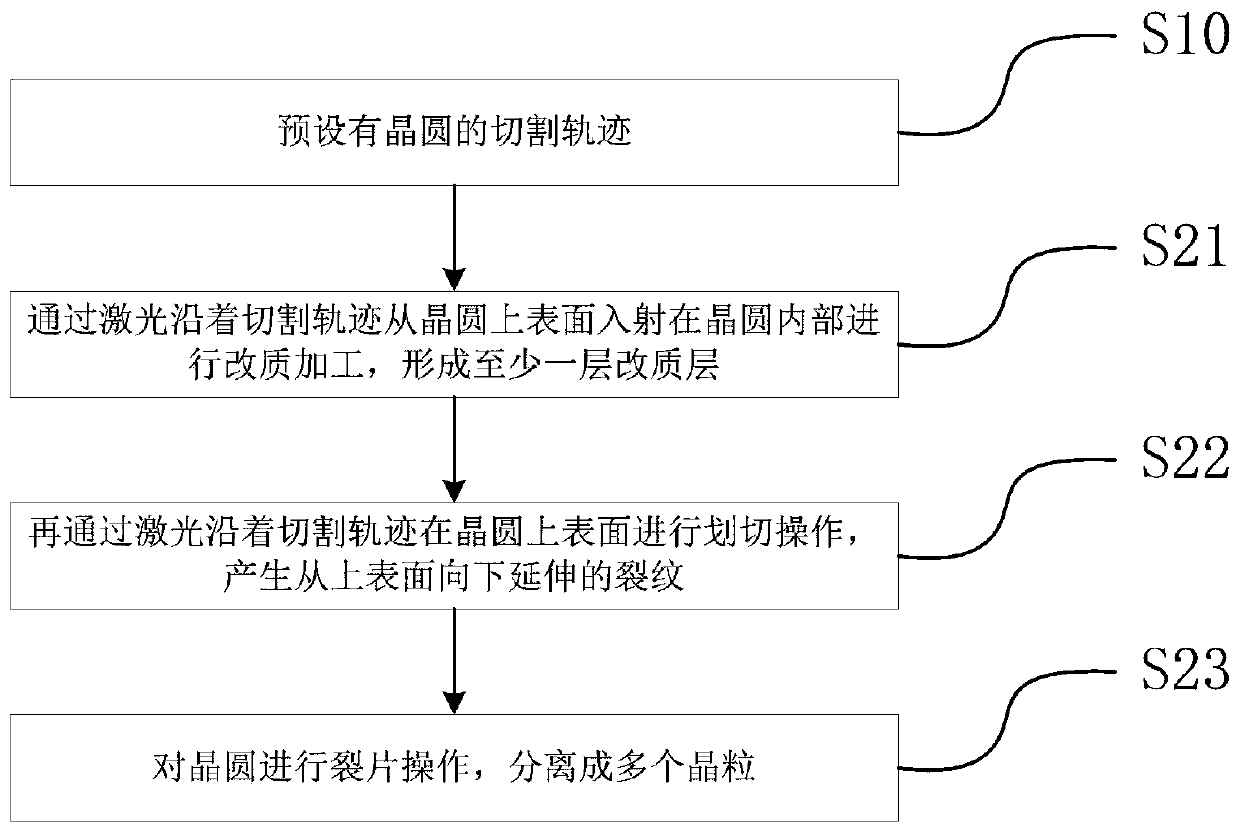
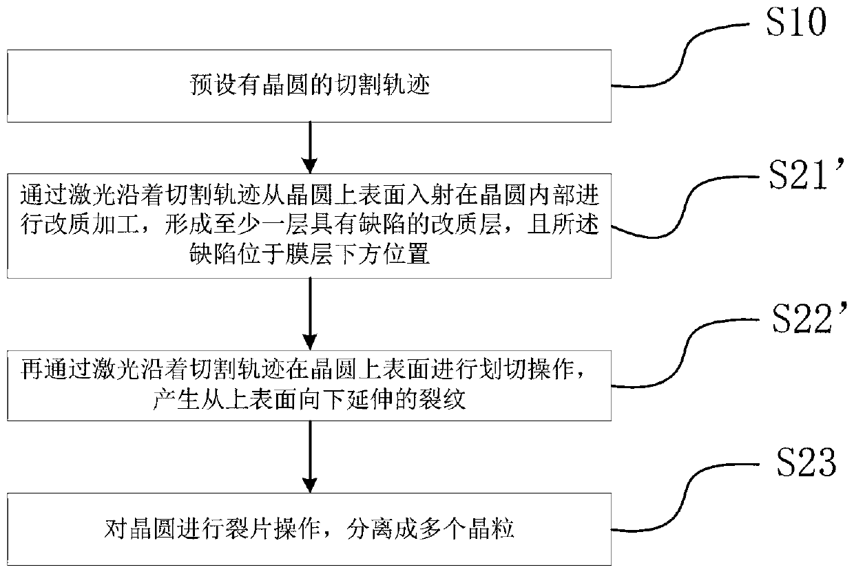
[0037] Step S10, the cutting track 101 of the wafer 100 is preset;

[0038] Step S21, using the laser to incident on the wafer 100 from the upper surface of the wafer along the cutting track 101 to perform modification processing to form at least one modification layer 120;

[0039] Step S22, performing a scribing operation on the upper surface 111 of the wafer 100 along the cutting track 101 with a laser to generate cracks 130 extending downward from the upper surface 111;

[0040] Step S23 , splitting the wafer 100 into multiple crystal grains 200 .

[0041] Specifically, provide a waf...


PUM


Abstract

The invention relates to the field of wafer machining, in particular to a laser machining method and system for a wafer. A wafer cutting track is preset. The laser machining method includes the stepsthat a laser is incident into the wafer to conduct modification machining from the upper surface of the wafer along the cutting track, and at least one modification layer is formed; then cutting-up operation is conducted on the upper surface of the wafer along the cutting track through the laser, and a crack extending downwards from the upper surface is generated; and piece splitting operation isconducted on the wafer, and the wafer is separated in to multiple grains. The laser machining method and system for the wafer are designed so that the problem of obvious edge breakage or even grain damage can be prevented in the piece separation process, and the piece separation yield and efficiency are improved under the condition that a cutting way is narrower or the function area of the cuttingway is plated with a film layer. Meanwhile, even if in the condition that the cutting way is not narrower or the film layer is not plated on the cutting way function area, the wafer piece separationyield and efficiency can still be improved in the scheme.

Description

technical field [0001] The invention relates to the field of wafer processing, in particular to a laser processing method and system for wafers. Background technique [0002] In the manufacturing process of semiconductor devices, on the surface of substrates such as silicon (Si) and silicon carbide (SiC), functional layers made of laminated insulating films and functional films are formed along the dicing lines (segmentation lines) arranged in a grid pattern. The area with optical devices is divided, and the wafer is cut to divide the devices of semiconductor wafers such as IC (Integrated Circuit) and LSI (Large-Scale Integration) into a matrix, thereby manufacturing individual semiconductor chips. [0003] In current manufacturing, wafer dicing generally uses three methods: [0004] 1. One is traditional mechanical cutting. Mechanical dicing mainly uses the mechanical stress of diamonds to grind wafers. There are problems such as mechanical deformation, stress concentrati...

Claims


Application Information

Patent Timeline
IPC IPC(8): B23K26/38B23K26/53
CPCB23K26/38B23K26/53
Inventor 王亭入余俊华黎国柱徐志军卢建刚李春昊巫礼杰尹建刚高云峰
Owner HANS LASER TECH IND GRP CO LTD
Why Eureka
Try Eureka