MSe2 thin film material and preparation method and application thereof
A thin film material and thin film technology, applied in the field of MSe2 thin film material and its preparation, can solve the problems of poor binding force, low preparation efficiency, and many operation steps, and achieve the effects of low friction coefficient, short preparation time and simple process
- Summary
- Abstract
- Description
- Claims
- Application Information
AI Technical Summary
Problems solved by technology
Method used
Image
Examples
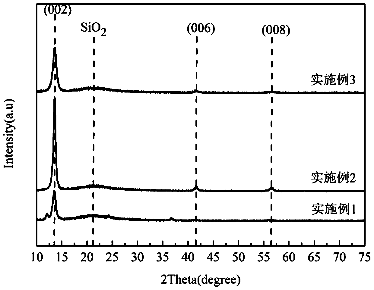
Embodiment 1
[0035] The invention provides a kind of MSe 2 The preparation method of film material, comprises the following steps:
[0036] (1) Stainless steel substrate pretreatment: use 500-mesh, 1000-mesh and 2000-mesh sandpaper to polish in sequence, and perform polishing treatment. The stainless steel is ultrasonically cleaned with acetone and absolute ethanol for 900s to remove surface impurities;
[0037] (2) RF magnetron sputtering tungsten diselenide thin film: After placing the pretreated stainless steel substrate obtained in step (1) in the magnetron sputtering chamber, vacuumize the magnetron sputtering chamber to 5.0×10 -4 Below Pa, use argon as the working gas, tungsten diselenide target as the sputtering source, control the pressure of argon to 0.5Pa, and perform radio frequency magnetron sputtering to generate non-stoichiometric diselenide on the surface of the stainless steel substrate Tungsten film (WSe x ,0≤x≤2);
[0038] RF magnetron sputtering parameters: the distan...
Embodiment 2
[0041] The invention provides a kind of MSe 2 The preparation method of film material, comprises the following steps:
[0042] (1) Stainless steel substrate pretreatment: use 500-mesh, 1000-mesh and 2000-mesh sandpaper to polish in sequence, and perform polishing treatment, and ultrasonically clean the stainless steel with acetone and absolute ethanol for 1200s respectively to remove surface impurities;
[0043] (2) RF magnetron sputtering tungsten diselenide thin film: After placing the pretreated stainless steel substrate obtained in step (1) in the magnetron sputtering chamber, vacuumize the magnetron sputtering chamber to 9.0×10 -4 Below Pa, use argon as the working gas, tungsten diselenide target as the sputtering source, control the pressure of argon to 2.0Pa, and perform radio frequency magnetron sputtering to generate non-stoichiometric diselenide on the surface of the stainless steel substrate Tungsten film (WSe x ,0≤x≤2);
[0044]RF magnetron sputtering parameters...
Embodiment 3
[0047] The invention provides a kind of MSe 2 The preparation method of film material, comprises the following steps:
[0048] (1) Stainless steel substrate pretreatment: use 500-mesh, 1000-mesh and 2000-mesh sandpaper to polish in sequence, and perform polishing treatment. The stainless steel is ultrasonically cleaned with acetone and absolute ethanol for 1500s to remove surface impurities;
[0049] (2) RF magnetron sputtering tungsten diselenide thin film: After placing the pretreated stainless steel substrate obtained in step (1) in the magnetron sputtering chamber, vacuumize the magnetron sputtering chamber to 3.0×10 -3 Below Pa, use argon as the working gas, tungsten diselenide target as the sputtering source, control the pressure of argon to 5.0Pa, and perform radio frequency magnetron sputtering to generate non-stoichiometric diselenide on the surface of the stainless steel substrate Tungsten film (WSe x ,0≤x≤2);
[0050] RF magnetron sputtering parameters: the dista...
PUM
| Property | Measurement | Unit |
|---|---|---|
| thickness | aaaaa | aaaaa |
| thickness | aaaaa | aaaaa |
Abstract
Description
Claims
Application Information
 - R&D Engineer
- R&D Manager
- IP Professional
- Industry Leading Data Capabilities
- Powerful AI technology
- Patent DNA Extraction
Browse by: Latest US Patents, China's latest patents, Technical Efficacy Thesaurus, Application Domain, Technology Topic, Popular Technical Reports.
© 2024 PatSnap. All rights reserved.Legal|Privacy policy|Modern Slavery Act Transparency Statement|Sitemap|About US| Contact US: help@patsnap.com


