Processing method, detection method and processing device of a silicon wafer

A processing method and processing device technology, applied in the direction of measuring devices, material inspection products, testing semiconductor materials, etc., can solve the problems that affect the accuracy of the observation and detection of silicon wafer surface defects, the amount of copper nitrate solution is difficult to control, and the distribution of copper is uneven. , to achieve the effect of easy determination and control, easy drying, and uniform copper distribution

Active Publication Date: 2022-03-25
XIAN ESWIN MATERIAL TECH CO LTD +1
View PDF12 Cites 0 Cited by
  • Summary
  • Abstract
  • Description
  • Claims
  • Application Information

AI Technical Summary

Problems solved by technology

[0004] In view of this, the present invention provides a processing method, a detection method and a processing device for silicon wafers, which are used to solve the problem that the amount of copper nitrate solution on the surface of silicon wafers is not easy to control, resulting in waste and a large amount of copper discharge pollution, uneven distribution of copper, and affecting silicon. Problems in Accuracy of Surface Defect Observation and Detection

Method used


Image

  • Processing method, detection method and processing device of a silicon wafer
  • Processing method, detection method and processing device of a silicon wafer

Examples


Embodiment Construction

[0038] In order to make the purpose, technical solutions and advantages of the embodiments of the present invention clearer, the technical solutions of the embodiments of the present invention will be clearly and completely described below with reference to the accompanying drawings of the embodiments of the present invention. Obviously, the described embodiments are some, but not all, embodiments of the present invention. Based on the described embodiments of the present invention, all other embodiments obtained by those of ordinary skill in the art fall within the protection scope of the present invention.

[0039] The processing method of the silicon wafer according to the embodiment of the present invention will be described in detail below.

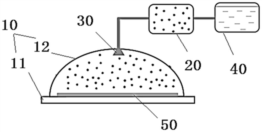
[0040] like figure 1 As shown, the method for processing a silicon wafer according to an embodiment of the present invention includes: atomizing a copper nitrate solution into an atomized gas and spraying it on the surface of the si...


PUM

PropertyMeasurementUnit
diameteraaaaaaaaaa

Abstract

The invention provides a treatment method, a detection method and a treatment device of a silicon wafer. The treatment method comprises: atomizing a copper nitrate solution into an atomized gas and spraying it on the surface of the silicon wafer to be treated; drying the surface of the silicon wafer; The finished silicon wafer is heat-treated to form decorations at defect sites on the surface of the silicon wafer. According to the processing method of the silicon chip of the present invention, the copper nitrate solution is atomized into an atomized gas and sprayed on the surface of the silicon chip to be treated, the surface of the silicon chip is dried, and the dried silicon chip is heat-treated to form a solid surface on the silicon chip. The defect position on the surface of the surface can be decorated, and the uniformity of the metal decoration can be greatly improved by the above method, and the measurement of metal pollution can be effectively controlled; and only a small amount of metal solution is used to avoid waste and heavy metal pollution; in addition, the release method The direct contact of personnel is avoided, and the safety is improved; and the surface of the silicon wafer is easy to dry, and the copper is evenly distributed, which improves the accuracy of the observation and detection of the surface defects of the silicon wafer.

Description

technical field [0001] The invention relates to the field of silicon wafer detection, in particular to a silicon wafer processing method, a detection method and a processing device. Background technique [0002] Nowadays, a detection method for surface crystal primary defects (COP) of Czochralski monocrystalline silicon wafers, especially large-sized monocrystalline silicon wafers (diameter 300mm and above) is the copper embellishment method, which uses heavy metal copper to embellish and Amplify the defects in the silicon wafer to facilitate subsequent observation and analysis, and microscopic defects at the nanometer level can be detected by the copper embellishment treatment on the surface of the silicon wafer. During the implementation of the method, the polished single crystal silicon wafer is directly dipped into the copper nitrate solution, and then the amount of heavy metal contamination on the surface is controlled by the dipping time and temperature, and the amount...

Claims


Application Information

Patent Timeline
Patent Type & Authority Patents(China)
IPC IPC(8): G01N33/00
CPCG01N33/00G01N2033/0095
Inventor 张婉婉文英熙柳清超
Owner XIAN ESWIN MATERIAL TECH CO LTD
Why Eureka
Try Eureka