Manufacturing method of semiconductor element
A manufacturing method and semiconductor technology, applied in semiconductor/solid-state device manufacturing, electrical components, circuits, etc., can solve problems such as weak adhesion, failure of etching and trenching, easy peeling off of photoresist, etc., to achieve excellent results and prevent tin liquid spillover effect
- Summary
- Abstract
- Description
- Claims
- Application Information
AI Technical Summary
Problems solved by technology
Method used
Image


Examples
Embodiment 1
[0026] A method for processing a semiconductor element, comprising the steps of:
[0027] (1) Pre-etching step:
[0028] 1) Coating the upper and lower sides of the semiconductor chip with photoresist;
[0029] 2) Covering the photoresist layer with a mask with a discontinuous line segment pattern for exposure and development;
[0030] 3) Putting the semiconductor chip into a mixed acid for pre-etching, the mixed acid is composed as follows by mass ratio: nitric acid: hydrofluoric acid: sulfuric acid: glacial acetic acid=5:8:2.5:4.8, nitric acid, hydrofluoric acid, sulfuric acid , The concentration ratio of glacial acetic acid is 5:5:2:5; the etching thickness is 25 μm.
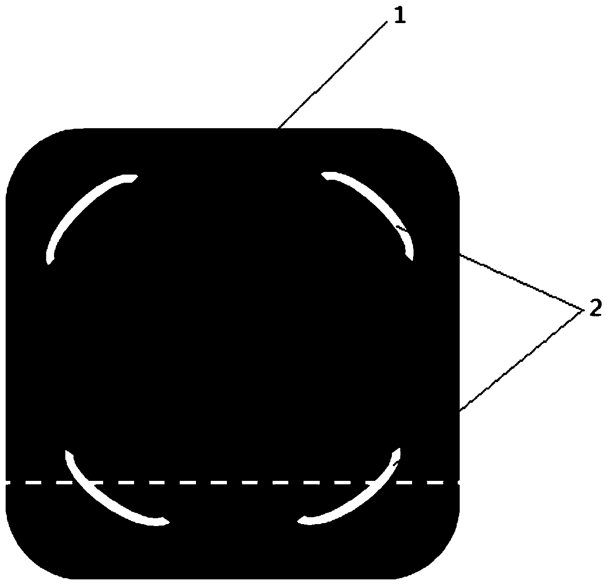
[0031] 4) After the etching is completed, remove the photoresist on the surface of the semiconductor chip, and dry the semiconductor chip; for the morphology after pre-etching, see figure 1 and figure 2 ;
[0032] (2) Conventional yellow light process steps:
[0033] The P-type surface and N-type surfa...
Embodiment 2
[0035] A method for processing a semiconductor element, comprising the steps of:
[0036] (1) Pre-etching step:
[0037] 1) Coating the upper and lower sides of the semiconductor chip with photoresist;
[0038] 2) Select a photomask with a strip-shaped closed ring pattern to cover the photoresist layer for exposure and development;
[0039] 3) Putting the semiconductor chip into a mixed acid for pre-etching, the mixed acid is composed as follows by mass ratio: nitric acid: hydrofluoric acid: sulfuric acid: glacial acetic acid=8:7:3:4, nitric acid, hydrofluoric acid, sulfuric acid , The concentration ratio of glacial acetic acid is 5:5:2:5; the etching thickness is 30 μm.
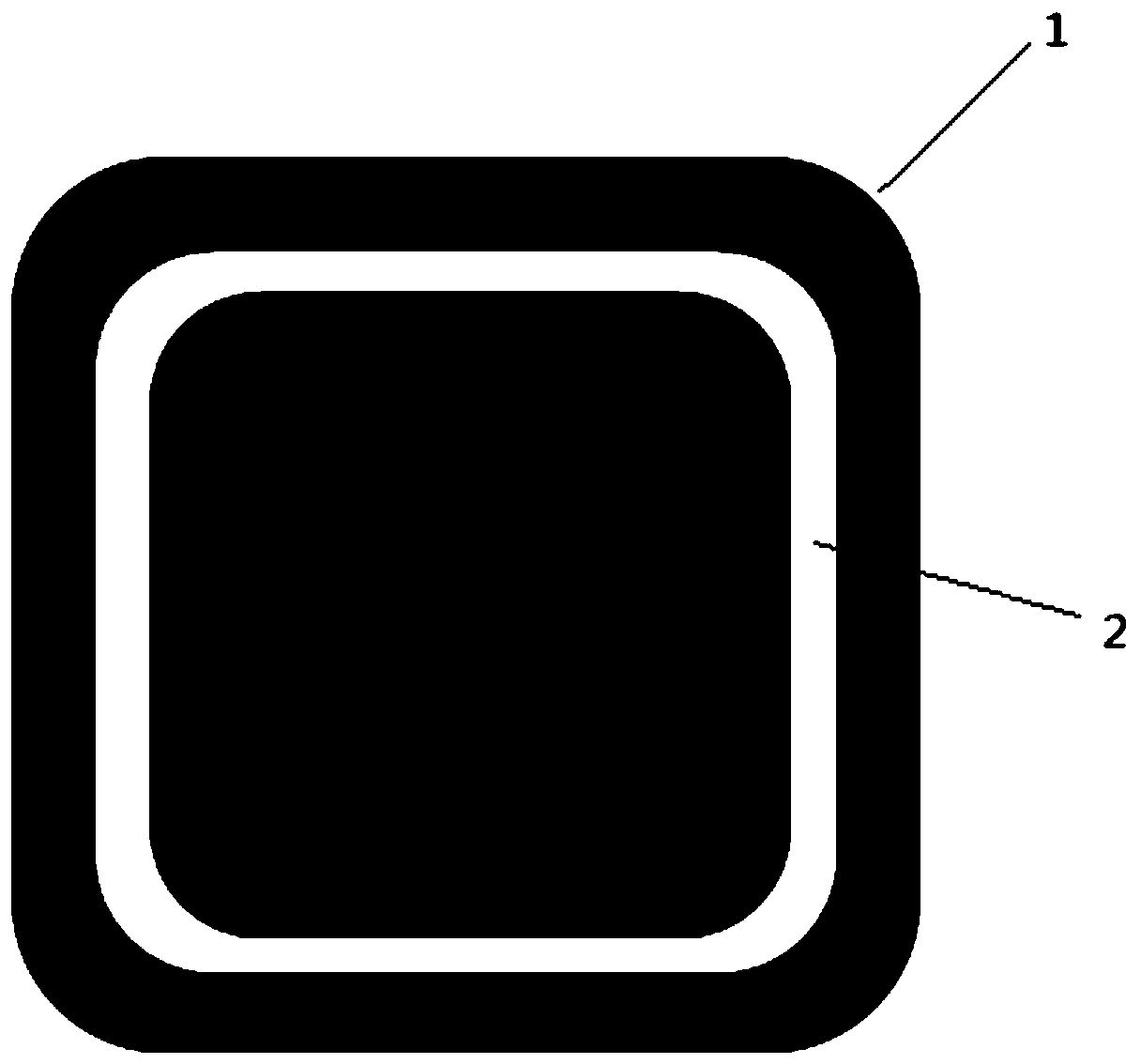
[0040] 4) After the etching is completed, remove the photoresist on the surface of the semiconductor chip, and dry the semiconductor chip; for the morphology after pre-etching, see image 3 ;
[0041] Other steps are with embodiment 1.
[0042] The semiconductor chip prepared by the method can effective...
Embodiment 3
[0044] A method for processing a semiconductor element, comprising the steps of:
[0045] (1) Pre-etching step:
[0046] 1) Coating the upper and lower sides of the semiconductor chip with photoresist;
[0047] 2) Select a photomask with a symmetrical triangle pattern to cover the photoresist layer for exposure and development;
[0048] 3) Putting the semiconductor chip into a mixed acid for pre-etching, the mixed acid is composed as follows by mass ratio: nitric acid: hydrofluoric acid: sulfuric acid: glacial acetic acid=8:8:3:5, nitric acid, hydrofluoric acid, sulfuric acid , The concentration ratio of glacial acetic acid is 5:5:2:5; the etching thickness is 35 μm.
[0049] 4) After the etching is completed, remove the photoresist on the surface of the semiconductor chip, and dry the semiconductor chip; for the morphology after pre-etching, see Figure 4 ;
[0050] Other steps are with embodiment 1.
PUM
 Abstract
Description
Claims
Application Information
 - R&D
- Intellectual Property
- Life Sciences
- Materials
- Tech Scout
- Unparalleled Data Quality
- Higher Quality Content
- 60% Fewer Hallucinations
Browse by: Latest US Patents, China's latest patents, Technical Efficacy Thesaurus, Application Domain, Technology Topic, Popular Technical Reports.
© 2025 PatSnap. All rights reserved.Legal|Privacy policy|Modern Slavery Act Transparency Statement|Sitemap|About US| Contact US: help@patsnap.com