High voltage-resisting thin film pressure sensor and preparation method thereof
A film pressure and high voltage technology, applied in the field of sensors, can solve the problems of easy current breakdown and low AC resistance, and achieve the effects of good insulation, strong AC resistance and strong chemical stability.
- Summary
- Abstract
- Description
- Claims
- Application Information
AI Technical Summary
Problems solved by technology
Method used
Image
Examples
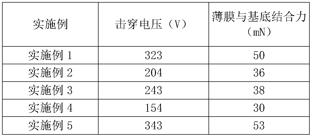
Embodiment 1
[0037] The acetophenone modified SiO of the present embodiment 2 The preparation method is as follows:
[0038] C1, take nano-SiO 2 100 grams of powder, add 400 grams of 0.2mol / L hydrochloric acid, and activate it for 5-10 minutes under stirring at 40r / min;
[0039] C2, then activate the SiO 2 Take out the powder, wash it with water for 3 times, remove the hydrochloric acid, add 250 g of 0.15 mol / L HF solution, heat to 60-70 °C under stirring at 60 r / min, and keep it for 15 min to obtain the mixed solution 1;
[0040] C3. Add 75 grams of 0.15 mol / L bromoacetophenone and 175 grams of 0.15 mol / L TBDPS solution to mixed solution 1, and heat to a temperature of 60-70° C. to obtain mixed solution 2;
[0041] C4. Filter the mixed solution 2 and dry it at 40-50°C to obtain acetophenone-modified SiO 2 .
[0042] The preparation method of the thin film pressure sensor of the present embodiment is as follows,
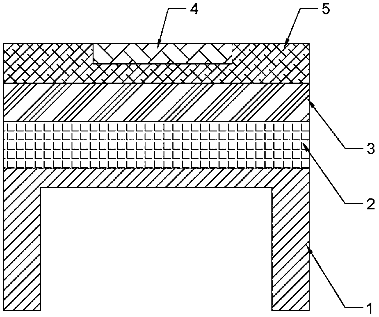
[0043] A1. Provide the substrate, the substrate is a stainless steel r...
Embodiment 2
[0047] Compared with embodiment 2, its difference is only that embodiment 2 uses common SiO 2 As an insulating layer, the specific operation steps for the preparation of its thin film pressure sensor are as follows:
[0048] A1. Provide the substrate, the substrate is a stainless steel rod, and the end face is round, and the precipitated acetophenone modified SiO 2 Before the thin film insulating layer, adjust the laser wavelength to 532nm, the laser pulse width to 10ns, the frequency to 1.5Hz, and the energy density to 1.5J / cm 2 , keep the sputtering pressure at 14Pa, carry out pre-sputtering for 4min, remove the surface contamination of the substrate, place the treated substrate in a vacuum chamber with a vacuum degree of 2Pa, adjust the distance between the laser target and the substrate to 30mm, and use a flowmeter to Into the vacuum chamber with a mass flow ratio of 30:60 of oxygen and argon with a concentration of more than 99% and a heating rate of 15-20°C / min to heat ...
Embodiment 3
[0052] Compared with Example 1, Example 3 differs only in that: Example 3 uses ion beam sputtering deposition technology to deposit acetophenone-modified SiO on the substrate. 2 Thin film insulation.
[0053] The specific operation steps of depositing the insulating layer are as follows:
[0054] S1. Set the ion energy of the argon ion beam generated by the main ion source to 500-800eV, and set the ion beam current density to 0.4-0.6mA / cm 2 ; and keep the background pressure of the vacuum chamber at 3×10⁻³Pa or below, and control the film deposition rate to 20-30nm / min; the rotation speed of the workpiece table is 7-9rpm, and the deposition angle is 45°;
[0055] S2. Use the argon ion beam generated by the main ion source to bombard the tantalum target on the target platform, so that the particles sputtered from the target react with the oxygen ion beam generated by the auxiliary ion source and deposit on the elastic substrate to form dioxide Tantalum base film;
[0056] S3...
PUM
| Property | Measurement | Unit |
|---|---|---|
| thickness | aaaaa | aaaaa |
| thickness | aaaaa | aaaaa |
| thickness | aaaaa | aaaaa |
Abstract
Description
Claims
Application Information
 - R&D Engineer
- R&D Manager
- IP Professional
- Industry Leading Data Capabilities
- Powerful AI technology
- Patent DNA Extraction
Browse by: Latest US Patents, China's latest patents, Technical Efficacy Thesaurus, Application Domain, Technology Topic, Popular Technical Reports.
© 2024 PatSnap. All rights reserved.Legal|Privacy policy|Modern Slavery Act Transparency Statement|Sitemap|About US| Contact US: help@patsnap.com


