Chemical amplification photoresist composition and application thereof in ultraviolet lithography
A composition and compound technology, applied in microlithography exposure equipment, photosensitive materials for optomechanical equipment, optics, etc., can solve problems such as insensitivity to light, lower resolution, rough line edges, etc., and achieve good roughness , high resolution, good line edge roughness
- Summary
- Abstract
- Description
- Claims
- Application Information
AI Technical Summary
Problems solved by technology
Method used
Image
Examples
Embodiment 1
[0034] Photoresist Composition 1: The host material is 35mg, the photoacid generator is 3.5mg, the solvent is propylene glycol methyl ether acetate 1mL.
[0035] Photolithography process conditions: after the surface of the silicon wafer is cleaned and activated by HMDS, the photoresist composition 1 is spin-coated on the silicon wafer, and soft-baked at 100°C for 180s. Interference exposure with 365nm laser at 2mW / s for 60s, post-baking condition at 70°C for 60s, developing condition as TMAH:H 2 O=2:1 develop for 10s, then rinse with water and blow dry with nitrogen.
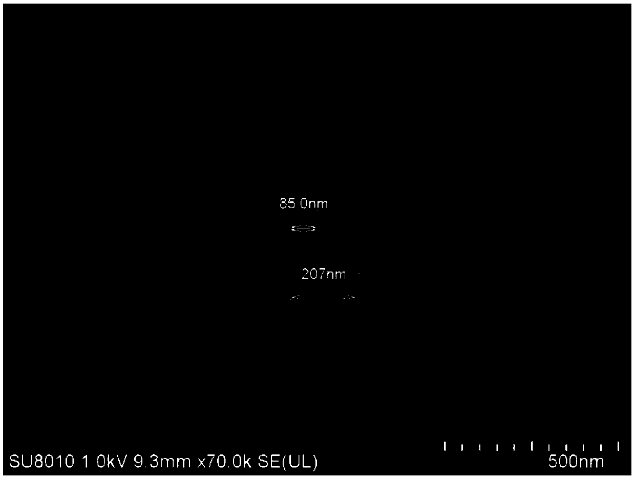
[0036] figure 1 It is the 365nm laser interference lithography pattern of the photoresist composition 1, and this formula can obtain a 85nm line width and better contrast ratio lithographic pattern under the 365nm laser interference lithography condition.
Embodiment 2
[0038] Photoresist Composition 2: Host Material 20mg, the photoacid generator is 2mg, the solvent is propylene glycol methyl ether acetate 1mL.
[0039] Photolithography process conditions: after the silicon wafer surface is cleaned and HMDS is activated, the photoresist composition 2 is spin-coated on the silicon wafer, and soft-baked at 100° C. for 180 s. Exposure to 365nm laser direct writing near-field, post-bake at 70°C for 20s, develop with TMAH for 60s, wash with water and dry with nitrogen.
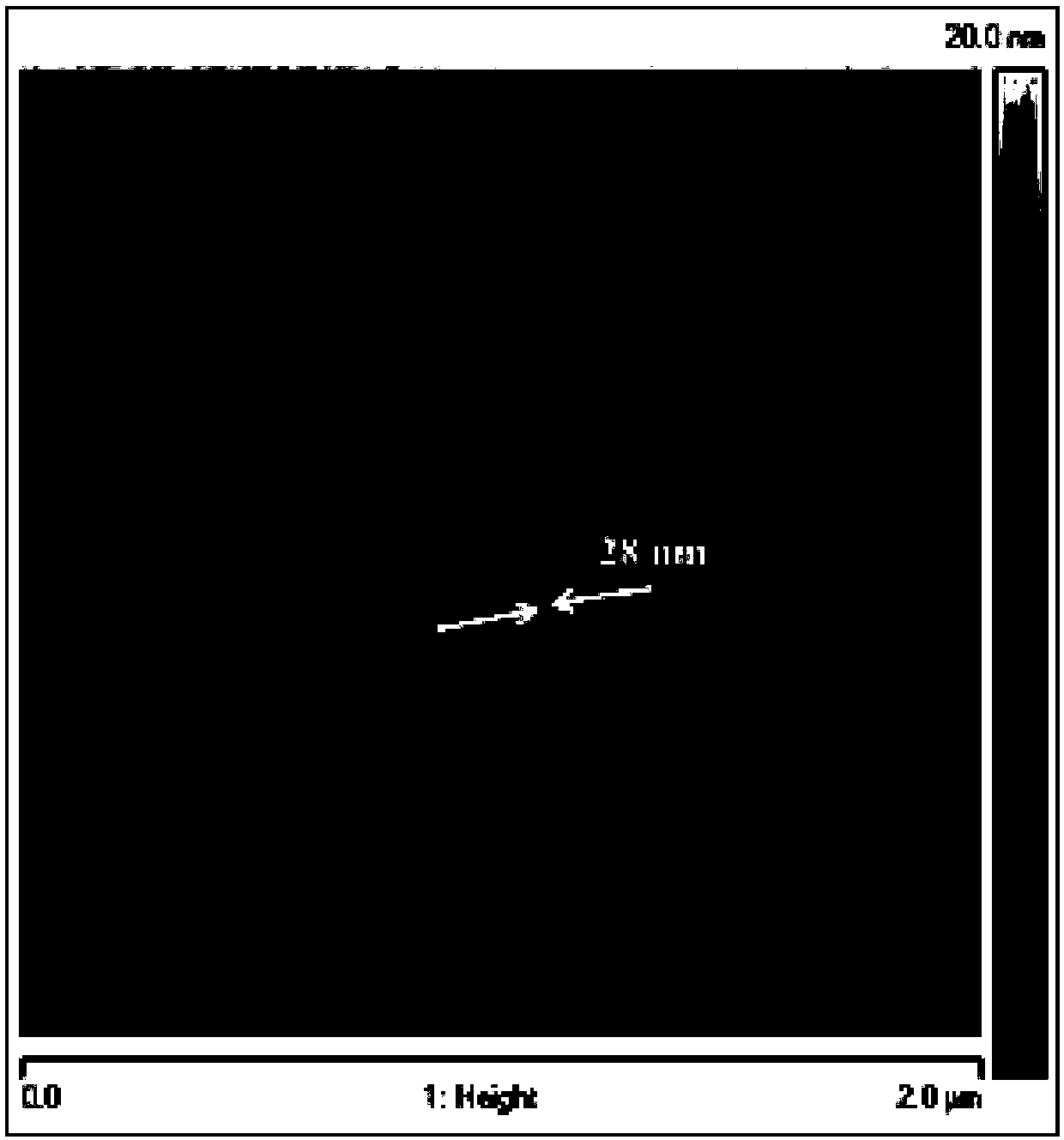
[0040] figure 2 For the photoresist composition 2, the laser direct writing near-field lithography pattern at 365 nm has a line width of 28 nm, which has exceeded the fine line width of the optical diffraction limit.
Embodiment 3
[0042] Photoresist composition 3:
[0043] The main material is 17.5mg, and 17.5 mg,
[0044] The photoacid generator is 3.5 mg, the anti-acid diffusing agent is tri-n-octylamine 0.35 mg, and the solvent is propylene glycol methyl ether acetate 1 mL.
[0045] Photolithography process conditions: after the surface of the silicon wafer is cleaned and activated by HMDS, the photoresist composition 3 is spin-coated on the silicon wafer, and soft-baked at 100° C. for 180 s. at 15mW / cm 2 Soft contact exposure on a UV exposure machine for 10s, post-baking conditions at 80°C for 60s, developing conditions as TMAH development for 60s, post-washing with nitrogen and drying.
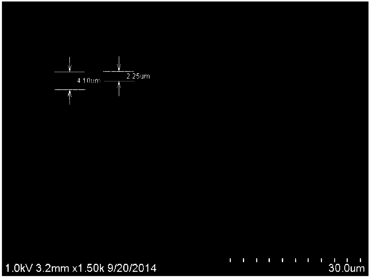
[0046] image 3 It is a lithographic image of a line width of 2 microns obtained by exposing the photoresist composition 3 on an ultraviolet exposure machine. The composition can be used in ultraviolet exposure machine lithography, the resolution can be distributed in the order of hundreds of nanometers t...
PUM
 Abstract
Description
Claims
Application Information
 - Generate Ideas
- Intellectual Property
- Life Sciences
- Materials
- Tech Scout
- Unparalleled Data Quality
- Higher Quality Content
- 60% Fewer Hallucinations
Browse by: Latest US Patents, China's latest patents, Technical Efficacy Thesaurus, Application Domain, Technology Topic, Popular Technical Reports.
© 2025 PatSnap. All rights reserved.Legal|Privacy policy|Modern Slavery Act Transparency Statement|Sitemap|About US| Contact US: help@patsnap.com


