Single-layer copper selenide two-dimensional atomic crystal material and preparation method and application thereof
A two-dimensional atomic crystal and copper selenide technology, applied in the field of nanomaterials, can solve the problems of few reports and difficulties in materials with a single-layer two-dimensional structure
- Summary
- Abstract
- Description
- Claims
- Application Information
AI Technical Summary
Problems solved by technology
Method used
Image

Examples
Embodiment 1
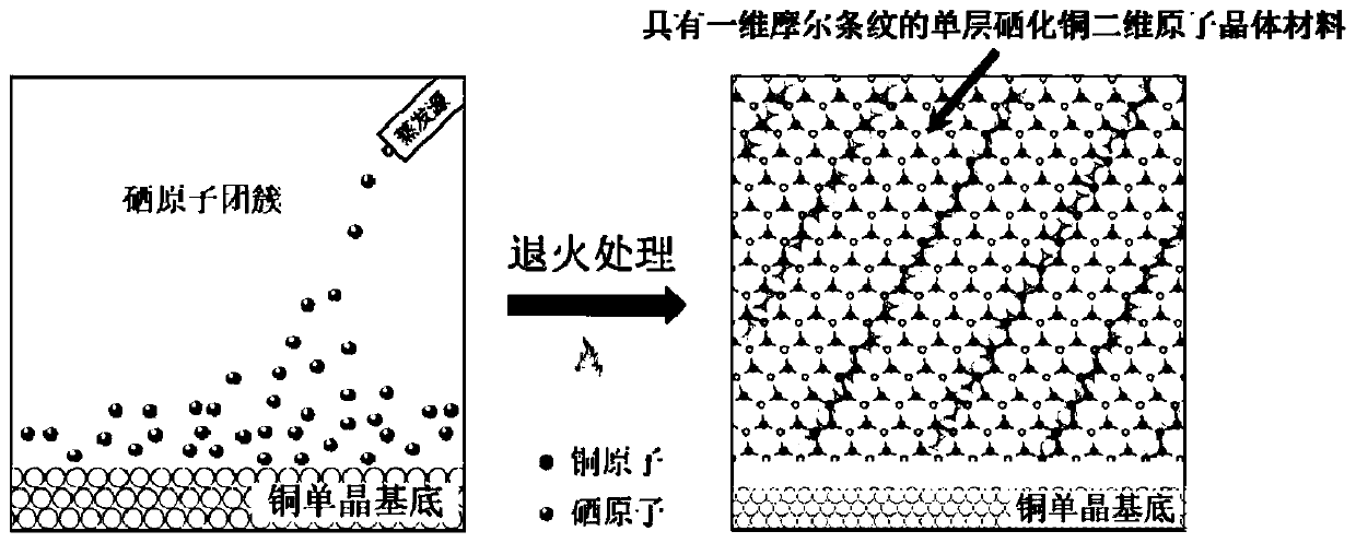
[0039] 1. Preparation of copper single crystal substrate
[0040] In an ultra-high vacuum chamber, an argon ion sputtering treatment is performed on the copper single crystal with an argon ion gun to obtain a copper substrate, and the copper substrate is heated and kept at 500° C. for 30 minutes to obtain a clean and flat copper single crystal substrate.
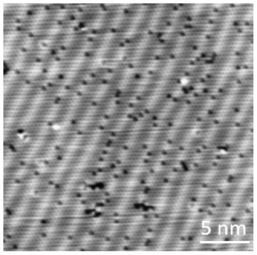
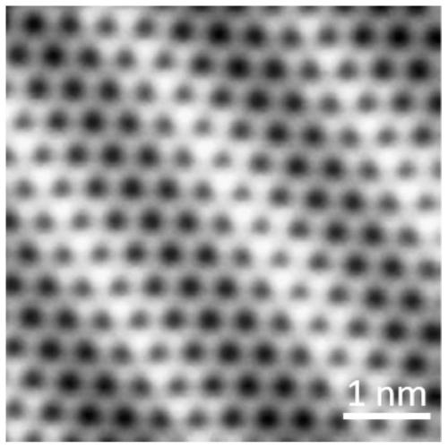
[0041] 2. Preparation of single-layer copper selenide two-dimensional atomic crystal material with one-dimensional moiré stripe structure
[0042] After preparing the copper single crystal substrate, in an ultra-high vacuum environment, using a thermal resistance k-cell molecular evaporation source, at an evaporation temperature of 125°C, evaporate and evenly deposit selenium atoms on the copper single crystal at 25°C On the surface of the substrate, the deposition time of selenium atoms is 20 minutes, and a single-layer copper selenide two-dimensional atomic crystal material with a one-dimensional moiré stripe structure is ...
Embodiment 2
[0044] 1. Preparation of copper single crystal substrate
[0045] In an ultra-high vacuum chamber, an argon ion sputtering treatment is performed on the copper single crystal with an argon ion gun to obtain a copper substrate, and the copper substrate is heated and kept at 500° C. for 30 minutes to obtain a clean and flat copper single crystal substrate.
[0046] 2. Preparation of single-layer copper selenide two-dimensional atomic crystal material with one-dimensional moiré stripe structure
[0047]After preparing the copper single crystal substrate, in an ultra-high vacuum environment, using a thermal resistance k-cell molecular evaporation source, at an evaporation temperature of 120°C, evaporate and evenly deposit selenium atoms on the copper single crystal at 30°C On the surface of the substrate, the deposition time of selenium atoms was 10 minutes. After the deposition is over, the copper single crystal substrate and the selenium atoms deposited on the surface of the co...
Embodiment 3
[0049] 1. Preparation of copper single crystal substrate
[0050] In an ultra-high vacuum chamber, an argon ion sputtering treatment is performed on the copper single crystal with an argon ion gun to obtain a copper substrate, and the copper substrate is heated and kept at 500° C. for 10 minutes to obtain a clean and flat copper single crystal substrate.
[0051] 2. Preparation of single-layer copper selenide two-dimensional atomic crystal material with one-dimensional moiré stripe structure
[0052] After preparing the copper single crystal substrate, in an ultra-high vacuum environment, using a thermal resistance k-cell molecular evaporation source, at an evaporation temperature of 125°C, evaporate and evenly deposit selenium atoms on the copper single crystal at 30°C On the surface of the substrate, the deposition time of selenium atoms is 15 minutes. During the deposition process, the copper single crystal substrate and selenium atoms are kept at a growth temperature of 30...
PUM
 Abstract
Description
Claims
Application Information
 - R&D
- Intellectual Property
- Life Sciences
- Materials
- Tech Scout
- Unparalleled Data Quality
- Higher Quality Content
- 60% Fewer Hallucinations
Browse by: Latest US Patents, China's latest patents, Technical Efficacy Thesaurus, Application Domain, Technology Topic, Popular Technical Reports.
© 2025 PatSnap. All rights reserved.Legal|Privacy policy|Modern Slavery Act Transparency Statement|Sitemap|About US| Contact US: help@patsnap.com