Semiconductor chip and manufacturing method thereof

a technology of semiconductor chips and manufacturing methods, applied in the field of semiconductor chips, can solve the problems of reducing the reliability of the semiconductor device manufactured, affecting the reliability affecting the quality of the semiconductor device, so as to improve the shear intensity of the indium-nickel alloy layer, improve reliability, and ensure the effect of precision

Inactive Publication Date: 2011-01-04
SONY CORP
View PDF6 Cites 10 Cited by
  • Summary
  • Abstract
  • Description
  • Claims
  • Application Information

AI Technical Summary

Benefits of technology

[0009]However, when the semiconductor chip 101 is mounted on the wiring board by the face down method, a break may occur in the intermediate metal compound layer 123. This may lower the reliability of the semiconductor device manufactured by mounting the semiconductor chip on the wiring board.
[0013]It is desirable to provide a semiconductor chip and a method of manufacturing thereof which allow a precise mounting of a semiconductor chip as well as an improvement of reliability.
[0020]Thus, the shear intensity of the intermediate metal compound layer is improved by forming the layer by alloying the indium layer and the copper layer containing copper atoms of not less than 0.5 atomic percent and not more than 5 atomic percent with respect to the indium atoms in the indium layer.
[0025]In the present invention, the indium layer and the nickel layer are alloyed to form the indium-nickel alloy layer having a thickness of 1 μm or more and including In7Ni3, whereby the shear intensity of the indium-nickel alloy layer is improved.
[0026]Accordingly, the present invention can provide the semiconductor chip and the method of manufacturing thereof which allow a precise mounting of the semiconductor chip as well as an improvement of reliability.

Problems solved by technology

However, when the semiconductor chip 101 is mounted on the wiring board by the face down method, a break may occur in the intermediate metal compound layer 123.
This may lower the reliability of the semiconductor device manufactured by mounting the semiconductor chip on the wiring board.

Method used


Image

  • Semiconductor chip and manufacturing method thereof
  • Semiconductor chip and manufacturing method thereof
  • Semiconductor chip and manufacturing method thereof

Examples


first embodiment

Configuration

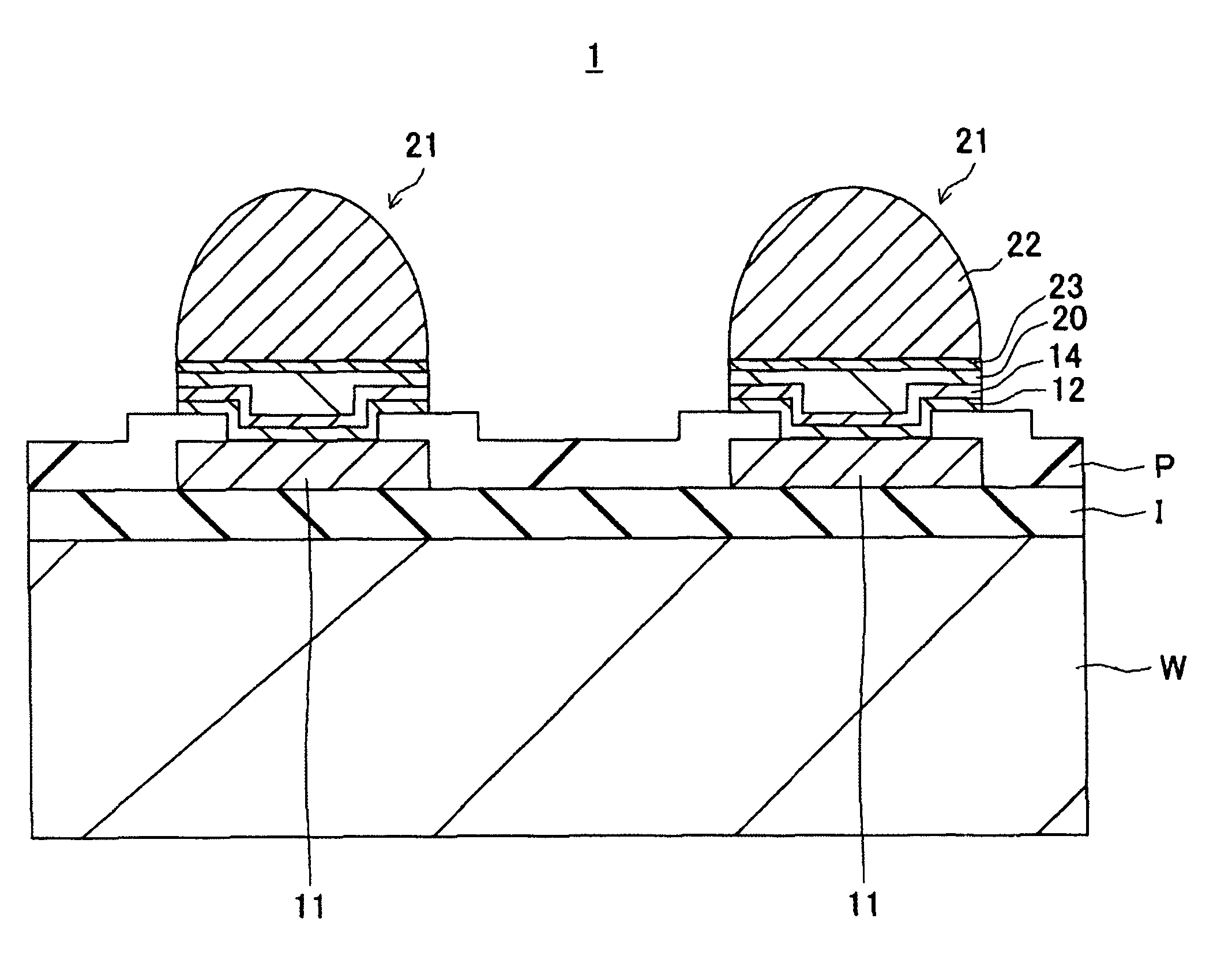
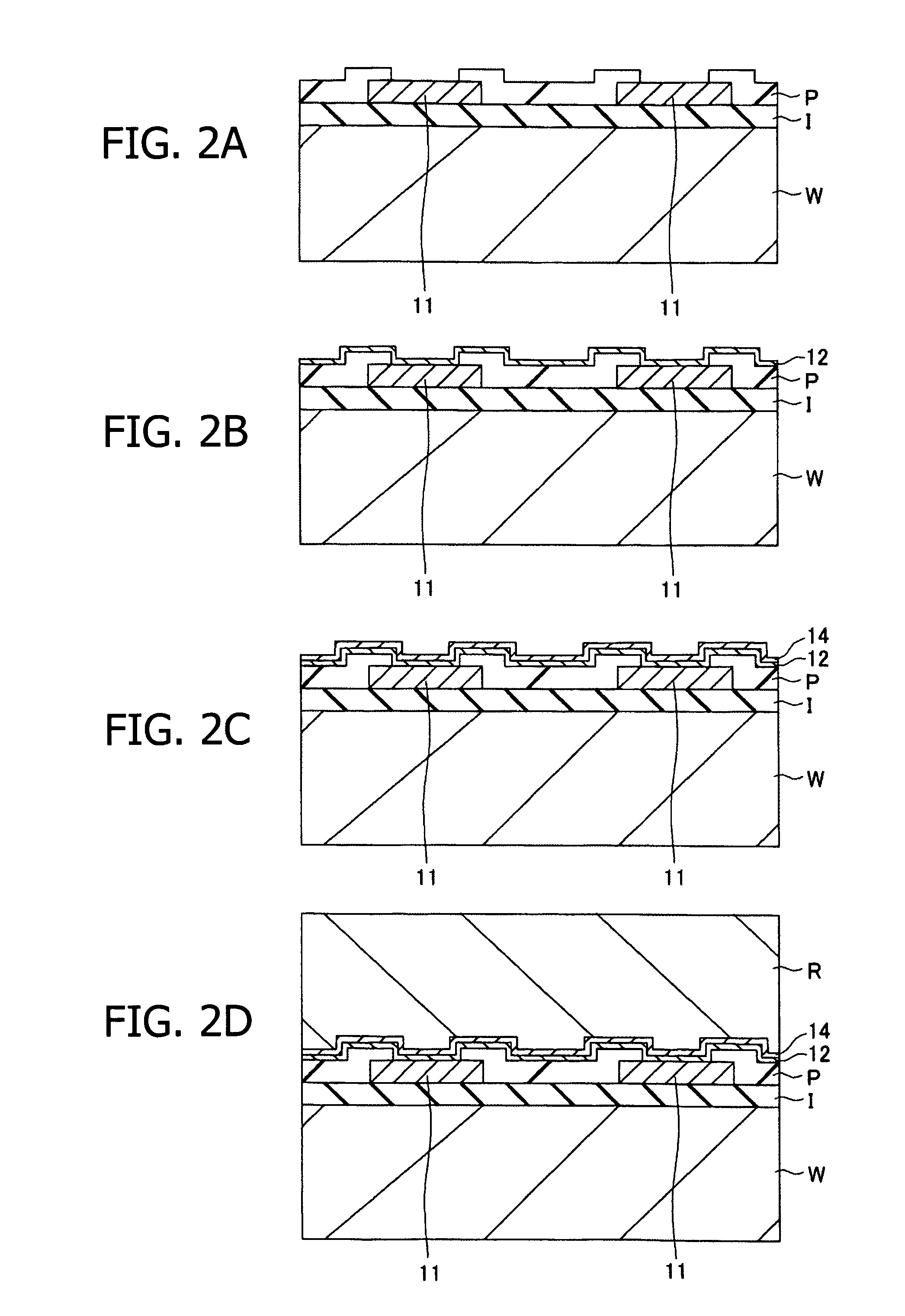
[0042]FIG. 1 is a sectional view showing parts of a semiconductor chip 1 in which a bump 21 is formed on a pad electrode 11 according to a first embodiment of the present invention.

[0043]As shown in FIG. 1, the semiconductor chip 1 has the pad electrode 11 and the bump 21, and the bump 21 is formed such that it corresponds to the pad electrode 11. A titanium layer 12 and a nickel layer 14 are sequentially laminated on the pad electrode 11 so as to cover the surface thereof. The bump 21 includes an indium layer 22 and an intermediate metal compound layer 23, composed of an indium-copper alloy layer interposed between the indium layer 22 and the nickel layer 14.

[0044]The respective components will be described sequentially.

[0045]The pad electrode 11 is made of, for example, aluminum and connected via an interlayer insulating film I to an electric circuit (not shown) formed on a wafer W of the semiconductor chip 1. As shown in FIG. 1, the surface of the pad electrode 11 is...

second embodiment

[0082]A second embodiment of the invention will be described below.

[0083]FIG. 5 is a sectional view showing parts of a semiconductor chip 1b in which a bump 21 is formed on a pad electrode 11 according to the second embodiment of the present invention.

[0084]As shown in FIG. 5, similarly to the first embodiment, the semiconductor chip 1b has the pad electrode 11 and the bump 21. Bump 21 is formed correspondingly to the pad electrode 11. A titanium layer 12, a copper layer 13, and a nickel layer 14 are sequentially laminated on the pad electrode 11 so as to cover the surface thereof. The bump 21 includes an indium layer 22, and an intermediate metal compound layer 23 is interposed between the indium layer 22 and the nickel layer 14.

[0085]In the semiconductor chip 1b of the second embodiment, the copper layer 13 underlies the nickel layer 14, and the nickel layer 14 has a thickness different from that in the first embodiment. Also, the intermediate metal compound layer 23 has a composi...


PUM

PropertyMeasurementUnit
thickaaaaaaaaaa
thicknessaaaaaaaaaa
thicknessaaaaaaaaaa

Abstract

A semiconductor chip formed with a bump such that the bump corresponds to a pad electrode. The pad electrode is covered with a nickel layer. The bump has an indium layer and an intermediate metal compound layer disposed between the indium layer and the nickel layer, and the intermediate metal compound layer is formed by alloying the indium layer and a copper layer containing copper atoms of not less than 0.5 atomic percent and not more than 5 atomic percent with respect to the indium atoms in the indium layer.

Description

BACKGROUND OF THE INVENTION[0001]1. Field of the Invention[0002]The present invention relates to a semiconductor chip and a manufacturing method thereof. In particular, the present invention relates to a semiconductor chip in which a bump is formed correspondingly to a pad electrode, and a method of manufacturing the semiconductor chip.[0003]2. Description of Related Art[0004]Instead of a wire bonding method, a face-down method is applied for densely mounting a semiconductor chip. In the face down method, the bump formed correspondingly to the pad electrode of the semiconductor chip is thermally compressed onto a terminal of a wiring board (for example, refer to Japanese Patent No. 2697116, Patent Document 1, and Japanese Unexamined Patent Application Publication No. 2000-349123, Patent Document 2).[0005]Specifically, the bump is formed on a substrate surface of the semiconductor chip such that the bump corresponds to the pad electrode provided on the substrate surface. The substrat...

Claims


Application Information

Patent Timeline
Patent Type & Authority Patents(United States)
IPC IPC(8): H01L23/48H01L29/40H01L23/52
CPCH01L23/49816H01L24/03H01L24/11H01L24/12H01L24/16H01L24/81H01L21/4853H01L24/75H01L2224/03912H01L2224/0401H01L2224/1147H01L2224/11901H01L2224/13099H01L2224/16H01L2224/75H01L2224/75301H01L2224/81203H01L2224/81801H01L2924/01004H01L2924/01005H01L2924/01013H01L2924/01014H01L2924/01015H01L2924/01022H01L2924/01028H01L2924/01029H01L2924/01033H01L2924/01049H01L2924/0105H01L2924/01061H01L2924/01074H01L2924/01075H01L2924/01078H01L2924/01079H01L2924/01082H01L2924/014H01L2924/00014H01L2224/13109H01L2924/01006H01L2924/01024H01L2224/0361H01L23/29
Inventor OZAKI, HIROSHIWAKIYAMA, SATORU
Owner SONY CORP
Why Eureka
Try Eureka