Solid state imaging device and manufacturing method thereof

Inactive Publication Date: 2009-02-19
FUJIFILM CORP
View PDF13 Cites 71 Cited by
  • Summary
  • Abstract
  • Description
  • Claims
  • Application Information

AI Technical Summary

Benefits of technology

[0035]According to the above manufacturing method, the upper mold die protects the upper face of the cover in the sealing step, and prevents the sealing resin to stick onto the cover. It is therefore possible to prevent the decrease in yield resulted from the stain of the cover caused by the sealing resin. Furthermore, the solid state imaging device except for the cover glass can be properly sealed. In addition, a plurality of solid state imaging devices can be manufactured at one time, and the cost will be reduced.
[0062]According to the present invention, it is possible to take the advantage of the CSP type solid state imaging device that it is small and to overcome the drawbacks of the through wirings and the side wirings, such as a high cost of manufacture, low reliability, and growth in chip size. Since the upper face of the cover for the sensor package will never be stained or damaged, the decrease of the yield is prevented and so does the rise in the price of the solid state imaging device. Additionally, it is possible to manufacture reliable system in packages at low cost.

Problems solved by technology

If the die attach material is paste or liquid and the thickness of coating is not accurately controlled, the cover glass are not level with each other on the circuit assembly board.
This may result to create a gap between the upper mold die and the cover glass, and the cover glass will be stained by the sealing resin.

Method used


Image

  • Solid state imaging device and manufacturing method thereof
  • Solid state imaging device and manufacturing method thereof
  • Solid state imaging device and manufacturing method thereof

Examples


first embodiment

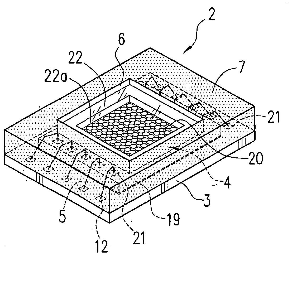
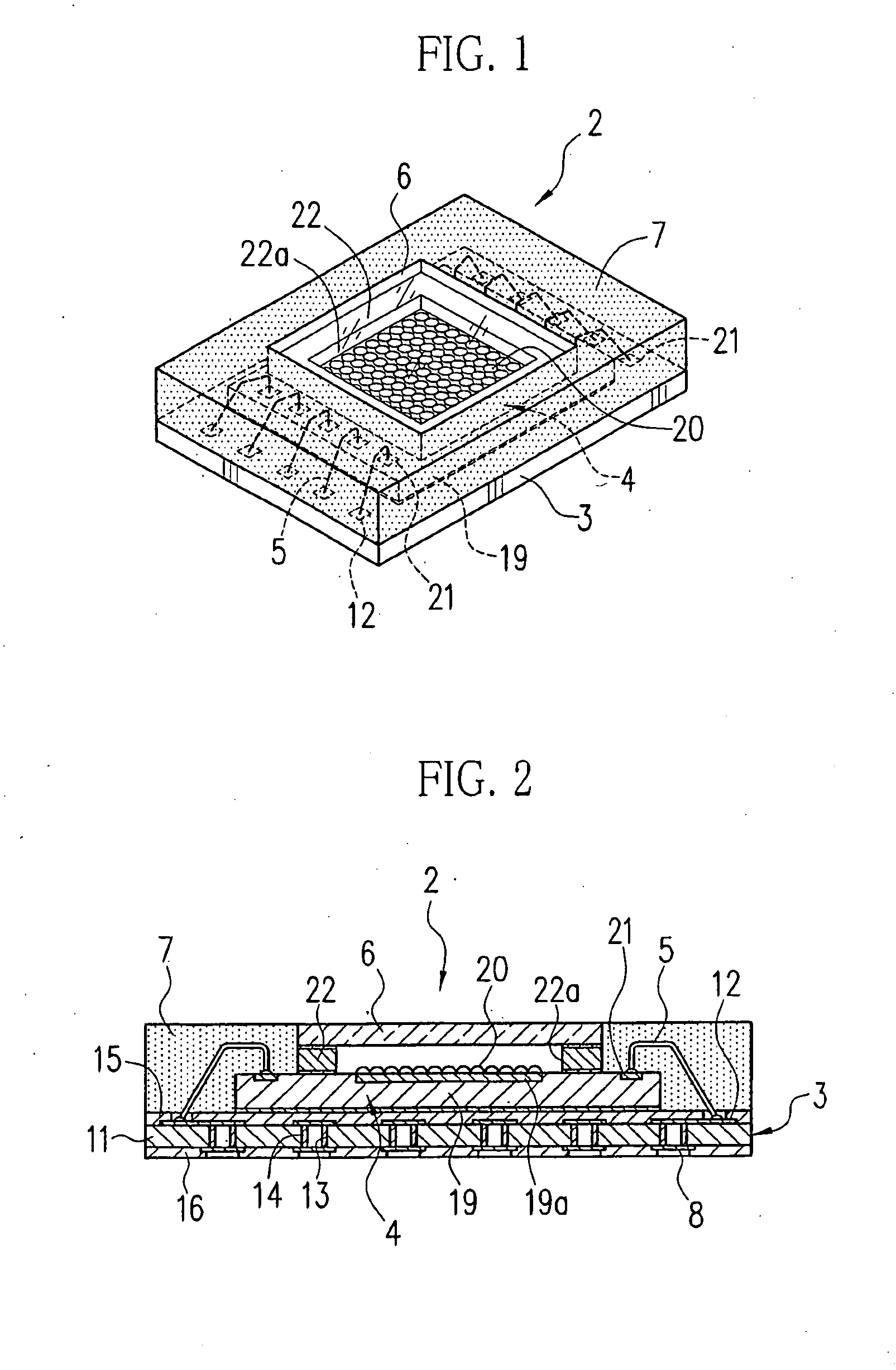
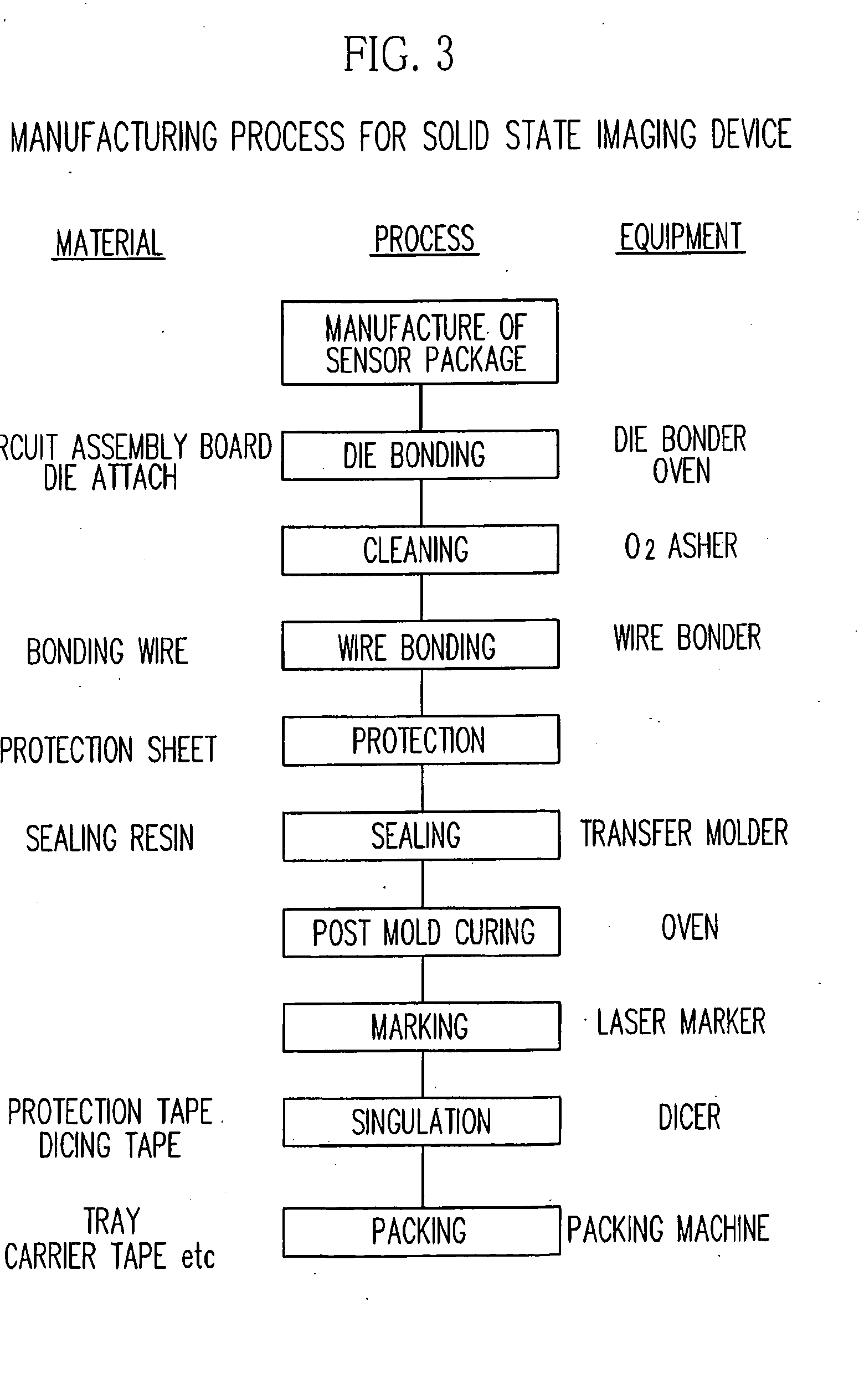
[0092]Referring now to FIG. 1 and FIG. 2, a solid state imaging device 2 of a first embodiment includes a rectangular circuit board 3, a sensor package 4 fixed onto the circuit board 3, a plurality of bonding wires 5 for connection between the circuit board 3 and the sensor package 4, sealing resin 7 that seals a periphery of a cover glass 6 of the sensor package 4, and external conductive pads 8 formed on the lower surface of the circuit board 3. The solid state imaging device 2 is in a package so called “Fine Pitch Land Grid Array (FLGA)”. The FLGA package is prevalent in the art, and it is possible to manufacture reliable solid state imaging devices 2 at low cost.

[0093]The circuit board 3 is a substrate board (or printed board) fabricated from a base 11 of glass epoxy or the like. On a top surface of the base 11, a plurality of internal conductive pads 12, i.e. internal electrodes, are formed for connection with the sensor package 4 through the bonding wires 5. Formed on an under...

second embodiment

[0129]Although the above embodiment is directed to the manufacturing method for the solid state imaging device in an FLGA package, the present invention is applicable to the solid state imaging device in a Fine Pitch Ball Grid Array (FBGA) package which uses solder balls as the external electrodes. As shown in FIG. 13 and FIG. 14, the solid state imaging device 78 of a second embodiment is provided with a solder ball 82 on each external conductive pads 81 of a circuit board 80, which is attached to a sensor package 79. The FBGA package is also prevalent in the art, and it is possible to manufacture reliable solid state imaging devices 78 at low cost.

[0130]To manufacture the solid state devices 78 in the FBGA packages, solder ball formation process are provided between the marking step and the singulation step, as shown by the flow chart of FIG. 15. The solder ball 82 is formed by, for example, a ball mounting method which includes a ball mounting step, a reflow step, and a cleaning ...

third embodiment

[0132]FIG. 16 and FIG. 17 show a solid state imaging device 85 of a Made from the lead frame, the solid state imaging device 85 is in a package called “Quad Flat Non-leaded (QFN)”. The solid state imaging device 85 is constituted of a die pad 87 to which a sensor package 86 is fixed, inner leads 90 as internal electrodes connected through bonding wires 88 to input / output pads 89 of the sensor package 86, and outer leads 92 as external electrodes exposed at lower side faces of sealing resin 91. The QFN package is prevalent in the art, and it is possible to manufacture reliable solid state imaging devices 85 at low cost. Although the under surface of the die pad 87 is covered with the sealing resin 91, it may be exposed for better heat radiation of the sensor package 86.

[0133]To manufacture the solid state imaging devices 85 in the QFN packages, a deburring step and a plating step are provided between the sealing step and the marking step, as shown by a flow chart of FIG. 18. In the ...


PUM


Abstract

A plurality of sensor packages (4) are fixed to a circuit assembly board (47) and placed on a lower mold die (56) of a transfer molding apparatus (54). Attached inside a cavity (58a) of an upper mold die (58) is a protection sheet (65), which will make contact with the upper face of a cover glass (6) of each sensor package (4). When the upper mold die (58) meshes with the lower mold die (56), the upper face of the cover glass (6) is tightly covered with the protection sheet (65). A plunger (62) is activated to fill the cavities (56a, 58a) with sealing resin (7). The upper face of the cover glass (6) is not stained or damaged when the peripheries of the sensor packages (4) are sealed.

Description

TECHNICAL FIELD[0001]The present invention relates to a manufacturing method of solid state imaging devices, and more particularly to a manufacturing method of a solid state imaging device with a resin sealed sensor package, and the resulting solid state imaging device.BACKGROUND ART[0002]Digital cameras and video cameras with a solid state imaging device of either CCD type or CMOS type are in widespread use. Often, the solid state imaging device, together with a memory device, is incorporated in electrical equipments such as personal computers, mobile phones, and personal digital assistances to provide them with an image capturing function. An increasing demand for the solid state imaging devices is downsizing so that it does not affect the size of the electrical equipments greatly.[0003]Solid state imaging device of chip scale package type (hereinafter “CSP”) are known in the art. The CSP type solid state imaging device is composed of, for example, an imaging chip provided with bo...

Claims


Application Information

Patent Timeline
IPC IPC(8): H04N5/335H01L21/02
CPCH01L21/561H01L24/97H01L21/6835H01L23/3121H01L25/0657H01L27/14618H01L27/14621H01L27/14627H01L27/14643H01L27/14683H01L27/14685H01L27/148H01L2224/48227H01L2224/48247H01L2224/48465H01L2224/8501H01L2224/85013H01L2924/01046H01L2924/01078H01L2924/01079H01L2924/15311H01L21/566H01L2224/32225H01L2224/73265H01L2924/10253H01L2224/97H01L2924/00H01L2224/85H01L23/544H01L2223/54433H01L2223/54486H01L2924/351H01L2924/15788H01L2924/12042H01L2924/181H01L2924/15183H01L2924/16195H01L2924/1815H01L2924/16235H01L2924/00012
Inventor NISHIDA, KAZUHIROSHIMAMURA, HITOSHITAKASAKI, KOSUKE
Owner FUJIFILM CORP
Why Eureka
Try Eureka