Electrode, thin film transistor (TFT), array substrate and display device
A technology for thin film transistors and array substrates, applied in the field of display devices, can solve the problems of unstable image signal transmission speed of displays, increased manufacturing cost of thin film transistors, poor image quality, etc., so as to avoid the diffusion of copper atoms and reduce the amount of overetching. , the effect of reducing damage
- Summary
- Abstract
- Description
- Claims
- Application Information
AI Technical Summary
Problems solved by technology
Method used
Image

Examples
Embodiment 1
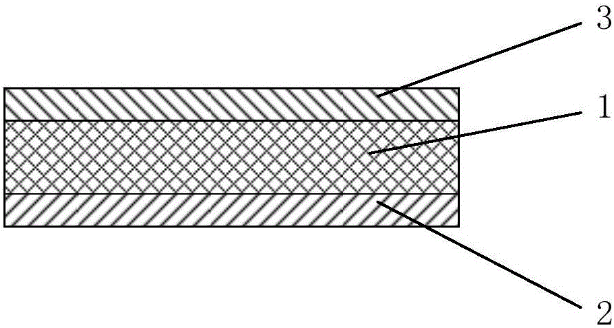
[0039] Such as figure 1 As shown, the embodiment of the present invention provides an electrode, which includes a copper electrode 1, a diffusion barrier layer 2 and an etching protection layer 3;
[0040] The diffusion barrier layer 2 and the etching protection layer 3 are arranged on both sides of the copper electrode 1 respectively, and both the diffusion barrier layer 2 and the etching protection layer 3 are made of zinc-based oxynitride.
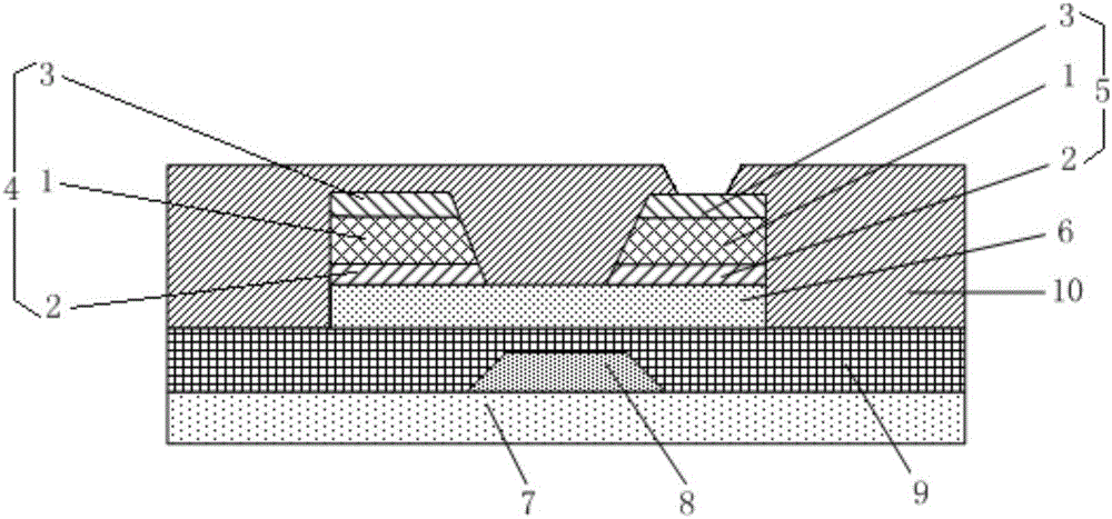
[0041] Electrode among the present invention comprises copper electrode 1, diffusion barrier layer 2 and etching protective layer 3, as figure 2 As shown, using this electrode as the source electrode 4 and the drain electrode 5 of the thin film transistor can reduce the resistance of the source electrode 4 and the drain electrode 5 of the thin film transistor, ensure that the image signal transmission speed of the display is stable, and the image quality is high, avoiding Driver circuits are installed on both sides of the thin film tr...
Embodiment 2
[0046] Such as figure 2 As shown, the embodiment of the present invention provides a thin film transistor, the source 4 and the drain 5 of the thin film transistor are the electrodes described in the first embodiment, and the diffusion barrier layer 2 and the thin film of the source 4 and the drain 5 The channel layer 6 of the transistor is contacted.
[0047] Since the electrodes in this embodiment include all the content in Embodiment 1, the same content will not be repeated here.
[0048] Electrode among the present invention comprises copper electrode 1, diffusion barrier layer 2 and etching protective layer 3, use this electrode as source 4 and drain 5 of thin film transistor, can reduce the source electrode 4 of thin film transistor and drain 5 resistance, to ensure that the image signal transmission speed of the display is stable, and the image quality is high, avoiding the installation of drive circuits on both sides of the thin film transistor to drive the electrode...
Embodiment 3
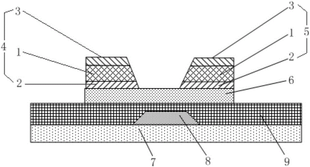
[0057] An embodiment of the present invention provides an array substrate including thin film transistors.
[0058] Since the thin film transistor in this embodiment includes all the content in the second embodiment, the same content will not be repeated here.
[0059] Electrode among the present invention comprises copper electrode, diffusion barrier layer and etching protection layer, uses this electrode as the source electrode and drain electrode of thin film transistor, can reduce the resistance of source electrode and drain electrode of thin film transistor, guarantees the image signal of display The transmission speed is stable, and the image quality is high, avoiding the installation of driving circuits on both sides of the thin film transistor to drive the electrodes, and reducing the manufacturing cost of the thin film transistor; On the other hand, both the diffusion barrier layer and the etching protection layer are made of zinc-based oxynitride, so as to avoid the ...
PUM
| Property | Measurement | Unit |
|---|---|---|
| Thickness | aaaaa | aaaaa |
Abstract
Description
Claims
Application Information
 - R&D
- Intellectual Property
- Life Sciences
- Materials
- Tech Scout
- Unparalleled Data Quality
- Higher Quality Content
- 60% Fewer Hallucinations
Browse by: Latest US Patents, China's latest patents, Technical Efficacy Thesaurus, Application Domain, Technology Topic, Popular Technical Reports.
© 2025 PatSnap. All rights reserved.Legal|Privacy policy|Modern Slavery Act Transparency Statement|Sitemap|About US| Contact US: help@patsnap.com