


Quick Research
Generate reliable direction feasibility study reports for your R&D in just a few steps.

Technical Q&A
Discover and master advanced knowledge NOW. Basics, ideas, possibilities, all at once.

Find Solutions
As an expert in R&D theories, this can generate solutions to your technical problems instantly.

Evaluate Feasibility
Analyze your overall solution with one click, know your potential R&D risks in advance.

Monitor Landscape
Get weekly tech updates, stay abreast of the latest tech innovations and key insights.
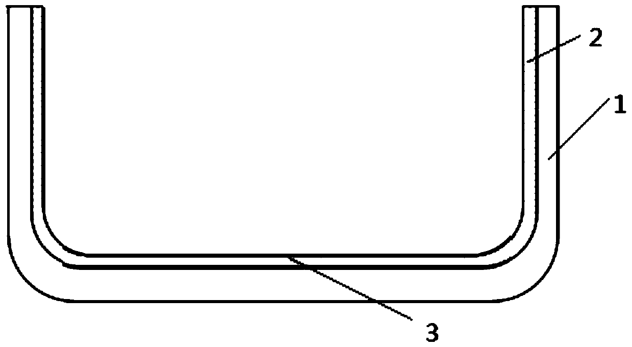
Novel ingot casting crucible sticking film and preparation method thereof
A crucible and ingot casting technology is applied in the field of new ingot casting crucible film and its preparation to achieve the effects of high conversion efficiency, improving purity and reducing impurities
- Summary
- Abstract
- Description
- Claims
- Application Information
AI Technical Summary
Problems solved by technology
Method used
Image


Examples
Embodiment 1
[0025] Electrophoresis deposition of the upper layer of silicon dioxide film containing Al powder
[0026] The specific solution components are ultrapure water, silica sol, high-purity silica, and Al powder. The slurry is prepared as follows: After weighting ultrapure water, silica sol, high-purity silica (purity of 99.999%, particle diameter of 10μm-20μm), and Al powder in a weight ratio of 100:1:5:0.1, First, put the ultrapure water, silica sol, and Al powder into a mixer and mix them evenly for 30 minutes to form a stable suspension, then mix with high-purity silicon dioxide particles and mix them evenly for 30 minutes and then stand for use.
[0027] When performing electrophoretic deposition of thin films, the process parameters are as follows: working voltage is 10-20V, working current is 4-5A, solution temperature is 80°C, and time is 30min.
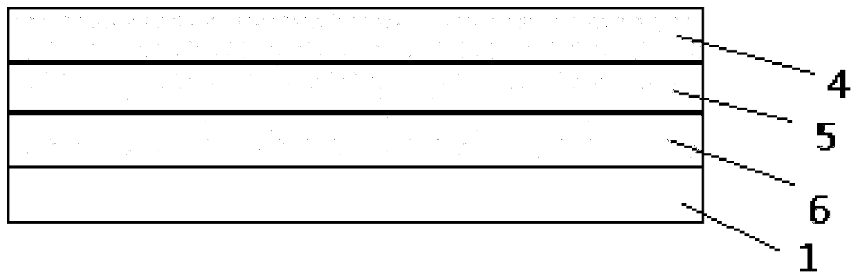
[0028] The made crucible film, the upper layer of the film is The film thickness of the uniformly aligned silica particles is 100μm, ...
Embodiment 2
[0036] Electrophoresis deposition of upper layer of silicon dioxide film containing Ni powder
[0037] The specific solution components are ultrapure water, silica sol, silica powder, and Ni powder. The preparation of the slurry is as follows: the ultrapure water, silica sol, silicon powder (particle diameter of 10μm-20μm), Ni powder in a weight ratio of 100:1:5:0.1 after the weight, the ultrapure water, silica sol , Ni powder is put into a mixer and stirred evenly for 30 minutes to form a stable suspension, then mixed with silicon powder (particle diameter is 10μm-20μm) and stirred evenly for 30 minutes and then stand for use.
[0038] When performing electrophoretic deposition of thin films, the process parameters are as follows: working voltage is 10-20V, working current is 4-5A, solution temperature is 80°C, and time is 30min.
[0039] The prepared crucible film has a silicon powder particle film thickness of 100 μm on the film, a carbon fiber structure film in the middle layer ...
Embodiment 3
[0047] Electrophoresis deposition of upper silicon dioxide film
[0048] The specific solution components are ultrapure water, silica sol, and high-purity silica. The slurry is prepared as follows: the ultrapure water, silica sol, high-purity silicon dioxide (purity of 99.999%, particle diameter of 10μm-20μm) in a weight ratio of 100:1:5, then the ultrapure water , The silica sol is put into a mixer and stirred evenly for 30 minutes to form a stable suspension, then mixed with high-purity silicon dioxide particles and stirred evenly for 30 minutes, and then set aside.
[0049] When performing electrophoretic deposition of thin films, the process parameters are as follows: working voltage is 10-20V, working current is 4-5A, solution temperature is 80°C, and time is 30min.
[0050] The prepared crucible film, the upper layer of the film is dense silica particles with a thickness of 100 μm, the middle layer of the film is a carbon fiber structure film with a thickness of 1 mm, and the ...
PUM
| Property | Measurement | Unit |
|---|---|---|
| diameter | aaaaa | aaaaa |
| thickness | aaaaa | aaaaa |
Abstract
Description
Claims
Application Information
 - R&D Engineer
- R&D Manager
- IP Professional
- Industry Leading Data Capabilities
- Powerful AI technology
- Patent DNA Extraction
Browse by: Latest US Patents, China's latest patents, Technical Efficacy Thesaurus, Application Domain, Technology Topic, Popular Technical Reports.
© 2024 PatSnap. All rights reserved.Legal|Privacy policy|Modern Slavery Act Transparency Statement|Sitemap|About US| Contact US: help@patsnap.com