Thin silicon-on-insulator (SOI) lateral insulator gate bipolar transistor (LIGBT) with folded groove gate
A folded groove and gate structure technology, applied to electrical components, circuits, semiconductor devices, etc., can solve the problems of long thermal process, large forward conduction voltage drop, large thermal budget, etc., and achieve high saturation operating current, small conduction The effect of low pass loss and low thermal budget
- Summary
- Abstract
- Description
- Claims
- Application Information
AI Technical Summary
Problems solved by technology
Method used
Image


Examples
Embodiment 1
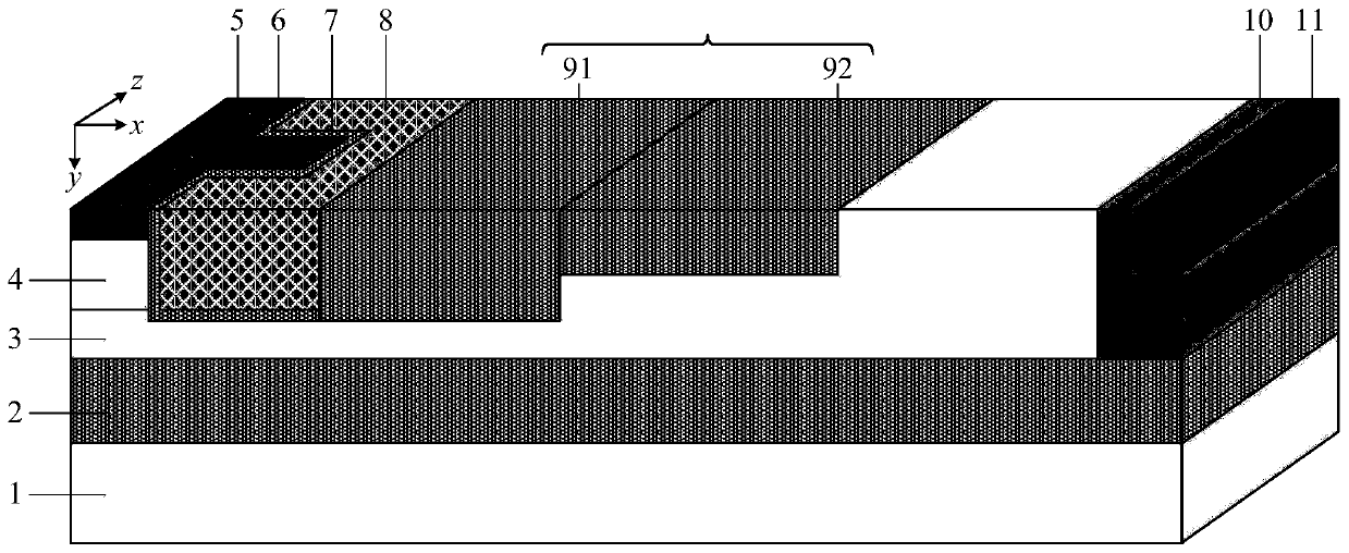
[0028] Such as figure 2 A kind of thin SOI LIGBT with folded groove gate is shown, comprising a substrate layer structure 1 arranged from bottom to top along the vertical direction of the device, a buried oxide layer structure 2 and an N-type top semiconductor layer structure 3; the surface of the top semiconductor layer structure Forming an emitter structure, a gate structure, a second insulating dielectric trench structure 9 of different depths, and a collector structure; the emitter structure includes a P-type well region 4 distributed along the vertical direction of the device, and the P-type well region 4 The upper P-type heavily doped region 5 and N-type heavily doped region 6; the bottom of the P-type well region is not in contact with the buried oxide layer structure 2; the P-type heavily doped region 5 and N-type heavily doped region 6 are in contact with each other; the upper surfaces of the P-type heavily doped region 5 and the N-type heavily doped region 6 jointly...
Embodiment 2
[0035] Such as image 3 As shown, the difference between this example and Example 1 is that the N-type heavily doped region 6 in this example is of the same "concave" type as the trench gate, and the P-type heavily doped region 5 is viewed along the vertical direction of the device as "T" shaped and complementary to the folded slot gate. Its working mechanism is the same as that of Embodiment 1. The P-type heavily doped region 5 distributed in a "T" shape increases the hole collection area, shortens the hole circulation path, and improves the anti-latch-up capability of the device.
Embodiment 3
[0037] Such as Figure 4 As shown, the difference between this example and Example 2 is that the P-type heavily doped region 5 in this example extends along the vertical direction of the device and has the same depth as the P-type well region 4 . Its working mechanism is the same as that of Embodiment 2, and the P-type heavily doped region 5 extending in the vertical direction accelerates the hole extraction speed during turn-off, which can improve the turn-off speed and anti-latch-up capability.
PUM
 Abstract
Description
Claims
Application Information
 - R&D
- Intellectual Property
- Life Sciences
- Materials
- Tech Scout
- Unparalleled Data Quality
- Higher Quality Content
- 60% Fewer Hallucinations
Browse by: Latest US Patents, China's latest patents, Technical Efficacy Thesaurus, Application Domain, Technology Topic, Popular Technical Reports.
© 2025 PatSnap. All rights reserved.Legal|Privacy policy|Modern Slavery Act Transparency Statement|Sitemap|About US| Contact US: help@patsnap.com