
Method for reducing surface defects of microstructured silicon-based photodetector and photodetector

A photodetector and microstructure technology, applied in the field of photodetection, can solve the problems of less suppression methods, affecting the performance of silicon-based detectors, affecting the performance characteristics of semiconductor materials, etc., to achieve the reduction of roughness, wide applicability and application potential, The effect of microstructural morphology improvement

Active Publication Date: 2020-07-03
CHANGCHUN INST OF OPTICS FINE MECHANICS & PHYSICS CHINESE ACAD OF SCI
View PDF2 Cites 0 Cited by
  • Summary
  • Abstract
  • Description
  • Claims
  • Application Information

AI Technical Summary

Problems solved by technology

[0002] The introduction of surface microstructures has been successfully applied as a technology to enhance the response of silicon-based detectors in the infrared band. Among them, the method of irradiating the sample surface with a femtosecond laser in a special atmosphere to form a surface microstructure is a very effective method. Near-infrared microstructure technology, the femtosecond laser irradiates the surface of the sample to form a microstructure in a special atmosphere, and a large number of pointed cone-shaped surface microstructures are formed on the silicon surface. At the same time, a supersaturated doped layer, microstructure morphology and supersaturated doped The impurity layer has a good effect on improving the response characteristics of silicon detectors in the near-infrared band, but the process of preparing the microstructure of the sample surface by femtosecond laser irradiation brings some defects in the silicon sample, and these defects affect the silicon-based detector. performance, such as dark current, carrier lifetime, etc.
[0003] The defect treatment of semiconductor materials has always been an important issue in the field of semiconductor materials, and its defects seriously affect the performance characteristics of semiconductor materials. However, there are few such defect suppression methods for new microstructured silicon-based optoelectronic materials. How to control them well It is of great significance to suppress and remove defects without damaging the microstructure morphology and the supersaturated doped layer

Method used


Image

  • Method for reducing surface defects of microstructured silicon-based photodetector and photodetector
  • Method for reducing surface defects of microstructured silicon-based photodetector and photodetector

Examples


Embodiment 1

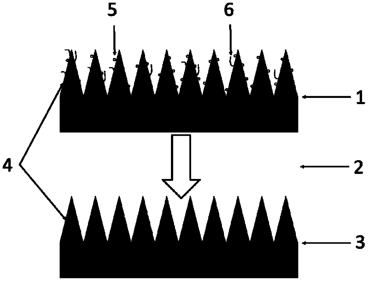
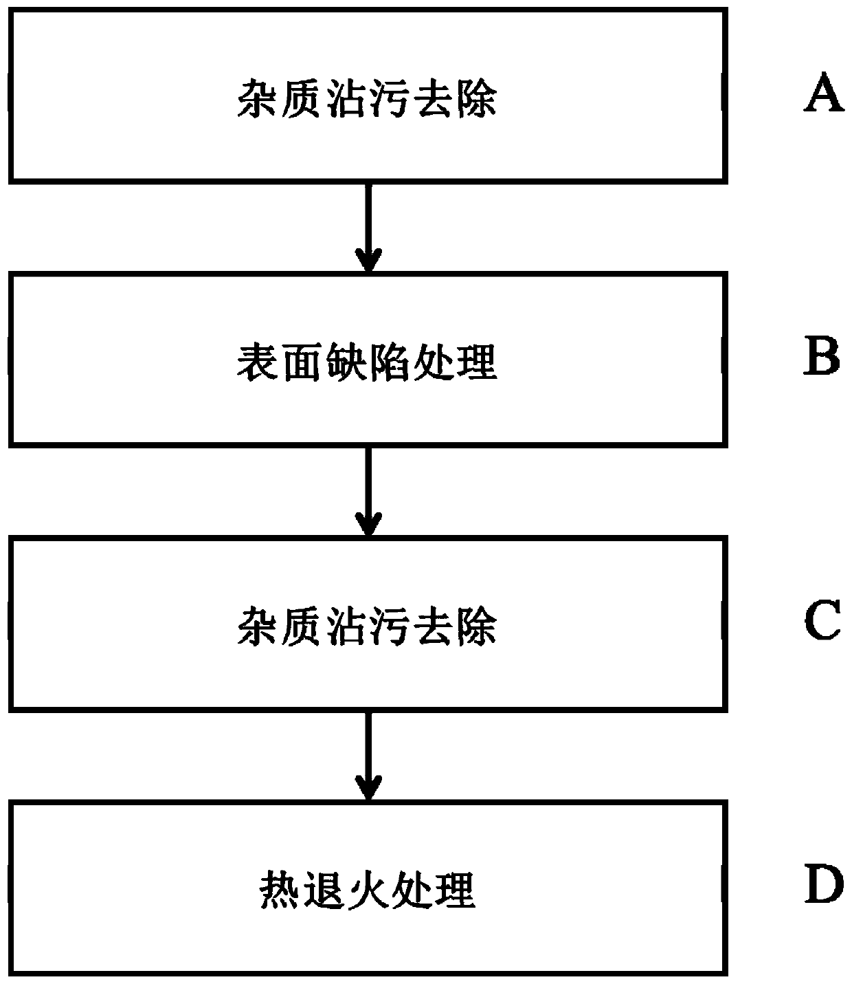
[0039] 1) with H 2 SO 4 :H 2 o 2 =1:3; the ratio of hydrofluoric acid corrosion inhibitor (1:20 ratio slow-release corrosion agent) is respectively configured with chemical cleaning agent and functional solvent;

[0040] 2) Place the microstructure silicon-based photodetector irradiated by the femtosecond laser in a special atmosphere in the H 2 SO 4 :H 2 o 2 = In the chemical cleaning agent with a ratio of 1:3, heat to 80 degrees for 15 minutes, take it out and rinse it with deionized water;

[0041] 3) Use hydrofluoric acid corrosion inhibitor (1:20 ratio slow-release corrosion agent) to remove the oxide layer on the surface of the microstructured silicon-based photodetector for 10 seconds;

[0042] 4) Perform RIE treatment on the microstructure silicon-based photodetector, the etching gas is SF6, the gas flow rate is 30sccm, the etching power is 30W, and the etching time is 60s;

[0043] 5) Use H 2 SO 4 :H 2 o 2 = 1:3 ratio of chemical cleaning agent to clean th...

Embodiment 2

[0046] 1) with H 2 SO 4 :H 2 o 2 =1:3; the ratio of hydrofluoric acid corrosion inhibitor (1:50 ratio slow-release corrosion agent) is respectively configured with chemical cleaning agent and functional solvent;

[0047] 2) Place the microstructure silicon-based photodetector irradiated by the femtosecond laser in a special atmosphere in the H 2 SO 4 :H 2 o 2 = In the chemical cleaning agent with a ratio of 1:3, heat to 80 degrees for 15 minutes, take it out and rinse it with deionized water;

[0048] 3) Use hydrofluoric acid corrosion inhibitor (1:50 ratio slow-release corrosion agent) to remove the oxide layer on the surface of the microstructured silicon-based photodetector for 5 to 10 seconds;

[0049] 4) Perform RIE treatment on the microstructure silicon-based photodetector, and the etching gas is NF 3 , the gas flow rate is 60sccm, the etching power is 50W, and the etching time is 30s;

[0050] 5) Use H 2 SO 4 :H 2 o 2 = 1:3 ratio of chemical cleaning agent...

Embodiment 3

[0053] 1) with H 2 SO 4 :H 2 o 2 =1:2; the ratio of hydrofluoric acid corrosion inhibitor (1:20 ratio slow-release corrosion agent) is respectively configured with chemical cleaning agent and functional solvent;

[0054] 2) Place the microstructure silicon-based photodetector irradiated by the femtosecond laser in a special atmosphere in the H 2 SO 4 :H 2 o 2 =In the chemical cleaning agent with a ratio of 1:2, heat to 80 degrees for 15 minutes, take it out and rinse it with deionized water;

[0055] 3) Use hydrofluoric acid corrosion inhibitor (1:20 ratio slow-release corrosion agent) to remove the oxide layer on the surface of the microstructured silicon-based photodetector for 10s;

[0056] 4) Perform RIE treatment on the microstructure silicon-based photodetector, and the etching gas is SF 6 , the gas flow rate is 60sccm, the etching power is 30W, and the etching time is 200s;

[0057] 5) Use H 2 SO 4 :H 2 o 2 = 1:2 ratio of chemical cleaning agent to clean th...


PUM

PropertyMeasurementUnit
currentaaaaaaaaaa

Abstract

The invention relates to the technical field of photoelectric detection, and specifically discloses a method for reducing surface defects of microstructured silicon-based photodetectors. The method of the invention comprises the steps of surface contamination removal, detector microstructure surface treatment process, detector surface contamination removal, device annealing process and the like. While reducing defects, the method of the present invention does not reduce the microstructure on the surface of the microstructured silicon-based photodetection device and the functional type of the supersaturated doped layer, and even has a certain improvement effect on the morphology of the microstructure, further reducing The roughness of the surface microstructure of the microstructured silicon-based photodetector is improved, so that the microstructured silicon-based photodetector device has better performance, and each step can be integrated with the existing CMOS process, which has a very wide range of applicability and application potential.

Description

technical field [0001] The invention relates to the technical field of photoelectric detection, in particular to a method for reducing surface defects of a microstructure silicon-based photodetector and the photodetector. Background technique [0002] The introduction of surface microstructures has been successfully applied as a technology to enhance the response of silicon-based detectors in the infrared band. Among them, the method of irradiating the sample surface with a femtosecond laser in a special atmosphere to form a surface microstructure is a very effective method. Near-infrared microstructure technology, the femtosecond laser irradiates the surface of the sample to form a microstructure in a special atmosphere, and a large number of pointed cone-shaped surface microstructures are formed on the silicon surface. At the same time, a supersaturated doped layer, microstructure morphology and supersaturated doped The impurity layer has a good effect on improving the res...

Claims


Application Information

Patent Timeline
Patent Type & Authority Patents(China)
IPC IPC(8): H01L31/18
CPCH01L31/186H01L31/1864Y02P70/50
Inventor 王延超王稞杨海贵王笑夷高劲松
Owner CHANGCHUN INST OF OPTICS FINE MECHANICS & PHYSICS CHINESE ACAD OF SCI
Learn More