A groove-type lateral pressure-resistant region with strontium titanate film

A technology of lateral withstand voltage and strontium titanate, which is applied in the direction of semiconductor devices, electrical components, circuits, etc., can solve the problem of low breakdown voltage, achieve high breakdown voltage and optimize the contradictory relationship

Active Publication Date: 2021-09-24
UNIV OF ELECTRONICS SCI & TECH OF CHINA
View PDF3 Cites 0 Cited by
  • Summary
  • Abstract
  • Description
  • Claims
  • Application Information

AI Technical Summary

Problems solved by technology

[0006] However, the surface electric field distribution in the existing groove-type withstand voltage region is strictly restricted by Poisson's equation after all. If the doping concentration of the semiconductor material is larger, the surface electric field distribution along the edge of the groove (including along the O 1 -O 2 Longitudinal electric field distribution, along the O 2 -O 3 The transverse electric field distribution, along the O 3 -O 4 The vertical electric field distribution) will be more inclined and uneven; under the same groove size, the breakdown voltage will be lower; this causes a contradictory relationship between the breakdown voltage and doping concentration in the withstand voltage region; because in a single The doping concentration in the pole device usually determines the on-resistance, so it also causes the contradiction between the device breakdown voltage and the on-resistance

Method used


Image

  • A groove-type lateral pressure-resistant region with strontium titanate film
  • A groove-type lateral pressure-resistant region with strontium titanate film
  • A groove-type lateral pressure-resistant region with strontium titanate film

Examples


Embodiment 1

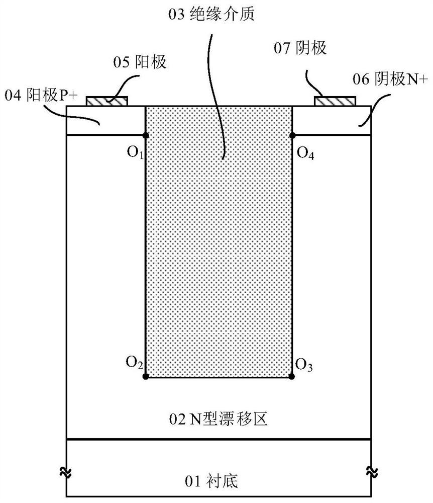
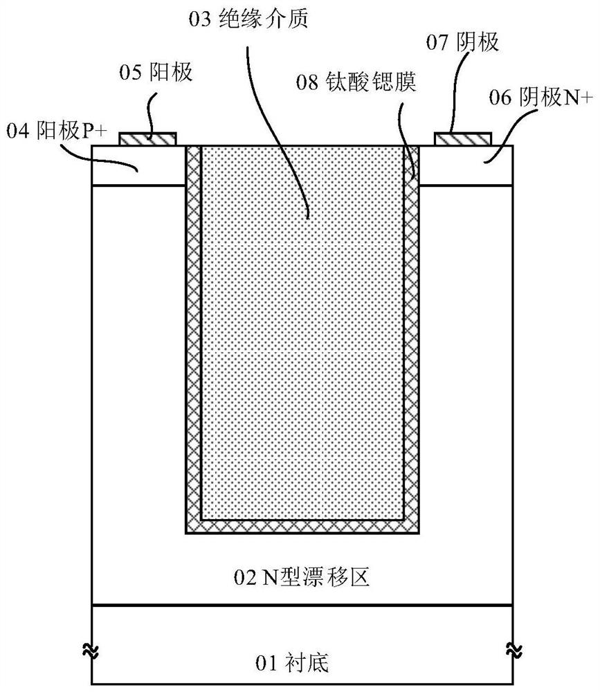
[0026] This embodiment provides a groove-shaped lateral pressure-resistant region with a strontium titanate film, the structure of which is as follows figure 2 Shown; including substrate (01), N-type drift region (02), insulating medium (03), anode P+ (04), anode (05), cathode N+ (06), cathode (07) and strontium titanate film (08); the N-type drift region (02) is located above the substrate (01); deep grooves are provided in the N-type drift region (02), and the insulating medium (03) is filled in the deep grooves; the anode P+ (04) is located above the N-type drift region (03) and on the left side of the insulating medium (04), and an anode (05) is arranged above the anode P+ (04); the cathode N+ (06) is located in the N-type drift region (03) Above and on the right side of the insulating medium (04), the cathode (07) is set above the cathode N+ (06); the strontium titanate film (08) is between the insulating medium (03) and the N-type drift region (02), the anode P+ ( 04) ...

Embodiment 2

[0030] This embodiment provides a groove-shaped lateral pressure-resistant region with a superjunction structure and a strontium titanate film, the structure of which is as follows Figure 4 shown; the difference from Example 1 is that the groove-type lateral voltage withstand region also includes a P-type drift region (09), and the P-type drift region (09) is arranged in the N-type drift region (03), Located under the anode P+ (04), and in contact with the anode P+ (04) and the strontium titanate film (08); the P-type drift region (09) is charged with the N-type drift region under the anode P+ (04) compensate.

[0031] The increase of the P-type drift region in this embodiment is conducive to the formation of a super junction structure under the anode P+, ​​which balances the charges that are difficult to be constrained by the new capacitance due to the proximity of the anode P+ in Example 1, thereby obtaining a more ideal electric field distribution.

[0032] With the help ...

Embodiment 3

[0036] This embodiment provides an N-channel LDMOS using a trench-type lateral withstand voltage region with a strontium titanate film, the basic structure of which is as follows Image 6 Shown; the structure uses a trench gate and SOI substrate.

[0037] The main manufacturing process of N-channel LDMOS using the existing groove-type lateral withstand voltage region includes steps such as wafer preparation, groove etching, insulating dielectric filling the groove, chemical mechanical polishing, and active region production, such as Figure 7 shown. In contrast, this embodiment only needs to deposit a certain thickness of strontium titanate material before depositing the insulating medium. Besides, no redundant mask or other operations are required, so no complicated process changes are caused.


PUM

PropertyMeasurementUnit
thicknessaaaaaaaaaa
dielectric strengthaaaaaaaaaa
thicknessaaaaaaaaaa

Abstract

The invention belongs to the field of semiconductor power devices, relates to a lateral withstand voltage region, and specifically provides a groove-shaped lateral withstand voltage region with a strontium titanate film, which is applied to junction edge terminals of semiconductor power devices or lateral semiconductor power devices including LDMOS (Lateral Double ‑Diffused MOSFET), LIGBT (Lateral Insulated Gate Bipolar Transistor); the present invention makes a part of the charges in the drift region act on the The strontium titanate film is used as the medium, and the anode and the drift region are the large capacitance of the two plates, which weakens the effect of the charge in the drift region on changing the surface electric field distribution, and can achieve a more ideal electric field distribution at the same doping concentration, or at the same Under the condition of breakdown voltage, the doping concentration is increased, and finally the contradictory relationship between breakdown voltage and on-resistance is optimized.

Description

technical field [0001] The invention belongs to the field of semiconductor power devices, and relates to a lateral voltage-resistant region, in particular a lateral voltage-resistant region with a groove structure; it can be applied to junction edge terminals of semiconductor power devices, or lateral semiconductor power devices include LDMOS (Lateral Double-Diffused MOSFET), LIGBT (Lateral Insulated Gate Bipolar Transistor), etc. Background technique [0002] Lateral semiconductor power devices, such as LDMOS (Lateral Double-Diffused MOSFET, LDMOS), etc., have been widely used in power integrated chips because of their characteristics of easy integration, easy driving, high withstand voltage, and low power consumption; but in high-voltage applications Among them, traditional LDMOS usually requires a very long lateral withstand voltage region to withstand high reverse withstand voltage, which occupies a large chip surface area and increases chip manufacturing costs. To this...

Claims


Application Information

Patent Timeline
Patent Type & Authority Patents(China)
IPC IPC(8): H01L29/78H01L29/40H01L29/06
CPCH01L29/063H01L29/407H01L29/7824H01L29/7825
Inventor 程骏骥陈为真林靖杰
Owner UNIV OF ELECTRONICS SCI & TECH OF CHINA
Why Eureka
Try Eureka