
Method for preparing hybrid integrated fiber optic gyroscope optical chip

A technology of optical chips and fiber optic gyroscopes, which is applied in gyroscope/steering sensing equipment, Sagnac effect gyroscopes, measuring devices, etc., can solve the problem of poor integration of semiconductor photonic devices, limitations of manufacturing process and semiconductor process compatibility Problems such as integration and miniaturization of the fiber optic gyroscope, poor system environmental adaptability and reliability, etc., to meet the requirements of reciprocity, low cost and high integration

Active Publication Date: 2019-04-05
TIANJIN JINHANG INST OF TECH PHYSICS
View PDF9 Cites 16 Cited by
  • Summary
  • Abstract
  • Description
  • Claims
  • Application Information

AI Technical Summary

Problems solved by technology

[0003] However, the existing fiber optic gyro system has certain technical defects: it is composed of some discrete components, each packaged, and the system is bulky; there are many optical fiber fusion points, which are prone to failure, and the system environment adaptability and reliability are poor; the cost is high, which is not conducive to engineering. Advanced production: each discrete component must be coupled with the device pigtail, with many and complex procedures, low coupling efficiency, and difficult to guarantee system repeatability
[0004] At present, the advanced interferometric fiber optic gyroscope optical system mainly includes superluminescent light-emitting diodes, fiber couplers, lithium niobate multifunctional integrated optical Y waveguide modulators, fiber optic rings, and photodetectors, which mainly rely on lithium niobate multifunctional integrated optical modulation. The chip is used to realize the phase modulation and optical beam splitter functions required by the inertial measurement system. However, due to the large bending loss of the lithium niobate waveguide, the inclination angle is usually between 3° and 5°, the size is large, and the manufacturing process is different from that of the optical beam splitter. The compatibility of semiconductor technology and its integration with semiconductor photonic devices are also poor, and the cost is also high, which limits the further integration and miniaturization of fiber optic gyroscopes

Method used


Image

  • Method for preparing hybrid integrated fiber optic gyroscope optical chip
  • Method for preparing hybrid integrated fiber optic gyroscope optical chip
  • Method for preparing hybrid integrated fiber optic gyroscope optical chip

Examples


preparation example Construction

[0064] In addition, the present invention also provides a preparation method for preparing the above-mentioned hybrid integrated fiber optic gyro optical chip, the method comprising the following steps:

[0065] Step 1: Design and cut out the substrate 1, the substrate of the lithium niobate Y-branch phase modulator 4 and the silicon substrate of the 3dB coupling 3 according to the above-mentioned chip size;

[0066] Step 2: Deposit a layer of SiO2 thin film on the silicon substrate by PECVD and ICP etching as a buffer layer; grow a germanium-doped SiO2 thin film on the SiO2 thin film, the thickness of which is the thickness of the waveguide core layer; Engraving and etching process forms a core layer waveguide pattern on the SiO2:Ge film; then deposits a layer of SiO2 film on it, and anneals to obtain a 3dB coupler;

[0067] Step 3: According to the graphic design of the above-mentioned lithium niobate Y-branch phase modulator 4, the Y-branch waveguide is fabricated on the li...

Embodiment 1

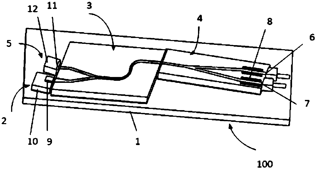
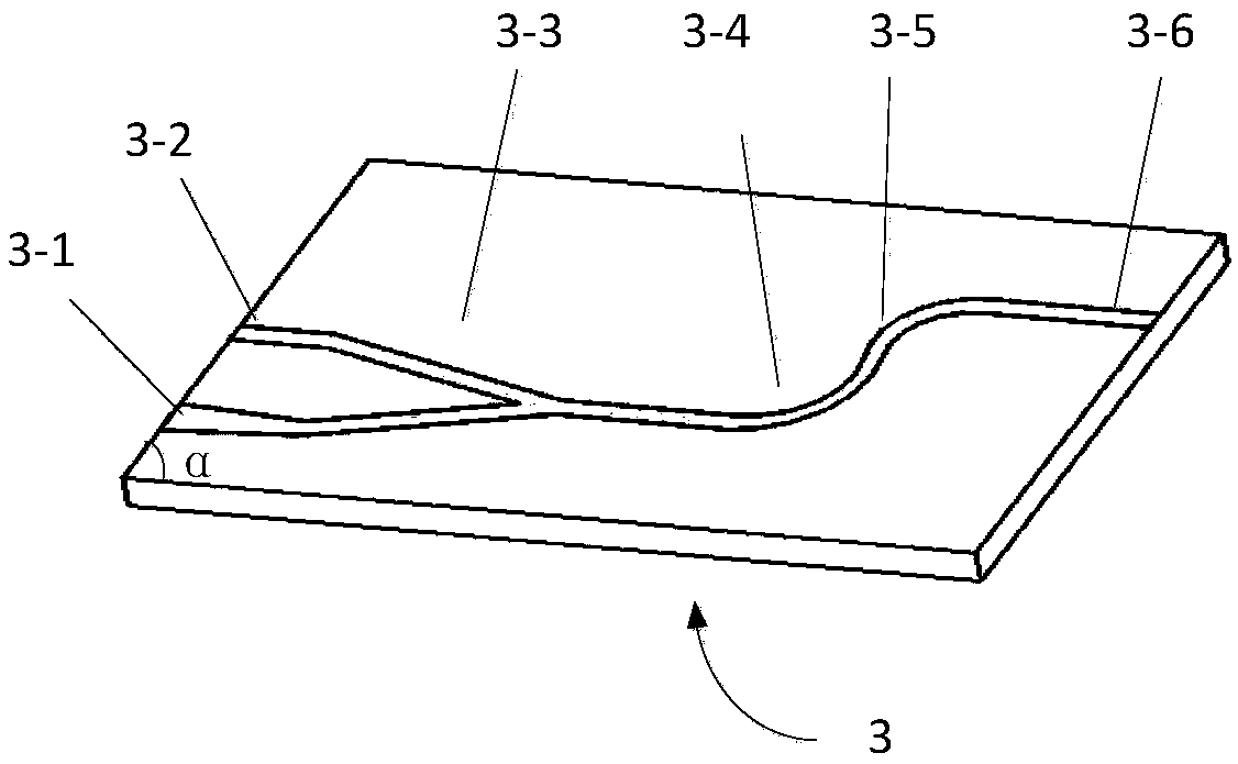
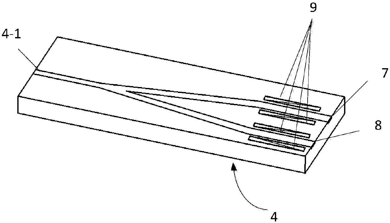
[0077] This example refers to Figure 1-3 , the hybrid integrated fiber optic gyroscope optical chip 100 of the present invention has a substrate 1, a light source 2, a 3dB coupler 3, a lithium niobate Y branch phase modulator 4, and a signal detector 5; the light source 2, the 3dB coupler 3, niobate The lithium Y-branch phase modulator 4 and the photodetector 5 are mixed and integrated on the substrate 1;

[0078] The lithium niobate Y-branch phase modulator 4 is a lithium niobate-based proton exchange waveguide. Taking the transmission wavelength of 1310nm as an example, the width of the single-mode waveguide is usually 5.5-6 μm;

[0079] Silicon-based 3dB coupler 3 is based on the mature silicon-based silicon dioxide optical waveguide manufacturing technology, usually using ion-enhanced chemical vapor deposition PECVD technology for SiO2 lower cladding and core film growth, and then using photolithography and inductively coupled plasma etching ICP technology forms a silicon-...


PUM

PropertyMeasurementUnit
Widthaaaaaaaaaa
Thicknessaaaaaaaaaa
Thicknessaaaaaaaaaa

Abstract

The invention belongs to the technical field of semiconductor processes, and in particular to a method for preparing a hybrid integrated fiber optic gyroscope optical chip. The chip comprises a substrate, a light source, a silicon-based 3dB coupler, a lithium niobate Y branch phase modulator and a signal detector, the silicon-based 3dB coupler is based on the silicon-based silicon dioxide opticalwaveguide technology and comprises a Y branch waveguide, two 90-degree circular arc waveguides, a tapered waveguide and two straight waveguides, which communicate with each other, a wide end of the tapered waveguide is used as an optical input port of the optical chip, the light source is aligned to the optical input port, the straight waveguide connected with a Y branch is used as a signal outputport of the optical chip, a photosensitive surface of the signal detector is aligned to the signal output port, and the straight waveguide connected with the 90-degree circular arc waveguide is usedas an optical transmission port and is spiced and fixed with a base waveguide end face of the lithium niobate Y branch phase modulator 3 through a waveguide coupling process. By adoption of the methodprovided by the invention, an optical fiber fusion point is removed, and the method has the advantages of high integration degree, small volume, low power consumption, good performance, good reliability and environmental adaptability, etc.

Description

technical field [0001] The invention belongs to the technical field of semiconductor technology, and in particular relates to a preparation method of a hybrid integrated fiber optic gyro optical chip. Background technique [0002] In many military and civilian applications such as aircraft and ship navigation, missile guidance, satellite orientation, geodesy, astronomical telescope observation and tracking, automotive GPS system-assisted navigation, and automotive autopilot, it is necessary to use small, high-reliability, and cheap inertial measurement devices. . Fiber optic gyroscope is an all-solid-state inertial instrument that uses the Sagnac effect to be sensitive to rotation or angular rate of rotation. It has light weight, low power consumption, low cost, long life, insensitive to acceleration, small size, no moving parts and good bias stability. It has better application prospects than laser gyro or other electromechanical gyroscopes due to its advantages such as sm...

Claims


Application Information

Patent Timeline
IPC IPC(8): G01C19/72
CPCG01C19/721
Inventor 张云霄孙文宝付振东康佳
Owner TIANJIN JINHANG INST OF TECH PHYSICS
Learn More