N-type LDMOS employing technology of reducing surface electric field

A surface electric field and technology technology, applied in circuits, electrical components, semiconductor devices, etc., can solve the problems of high specific on-resistance, low N-type LDMOS withstand voltage, etc., to improve breakdown voltage, reduce surface electric field, leakage, etc. The effect of high pressure resistance

Inactive Publication Date: 2019-03-01
TIANJIN UNIV
View PDF6 Cites 1 Cited by
  • Summary
  • Abstract
  • Description
  • Claims
  • Application Information

AI Technical Summary

Problems solved by technology

[0005] In order to solve the problems existing in the prior art, the present invention provides an N-type LDMOS using the technology of reducing the surface electric field to solve the problems of low withstand voltage and high specific on-resistance of the N-type LDMOS in the prior art

Method used


Image

  • N-type LDMOS employing technology of reducing surface electric field

Examples


Embodiment Construction

[0016] The present invention will be described in further detail below in conjunction with the accompanying drawings.

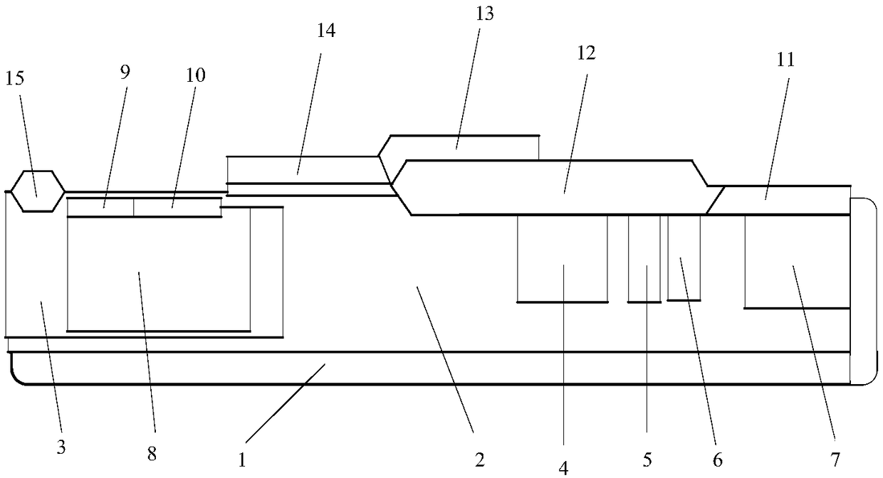
[0017] Such as figure 1 The present invention shows an N-type LDMOS using the technology of reducing the surface electric field, including a p-type substrate layer 1, the p-type sink layer 1 is formed by implanting boron ions in single crystal silicon, on the p-type substrate layer 1 The end face is a deep n well layer 2, the deep n well layer 2 is formed by implanting a large amount of phosphorus ions, and the deep n well layer 2 includes a deep p well layer 3, a p-type doped region 4, a first The drift ring 5, the second drift ring 6 and the n well layer 7, the deep p well layer 3 and the p-type doped region 4 are realized by implanting boron ions of different concentrations and energies, and the energy of the implanted ions is different to adjust The deep p well layer 3 includes a p well layer 8, the function of the p well layer 8 is to reduce the parasit...


PUM


Abstract

The invention discloses an N-type LDMOS employing a technology of reducing a surface electric field. The N-type LDMOS comprises a p-type substrate layer, wherein a deep N well layer is arranged at anupper end surface of the p-type substrate layer, a deep p well layer, an n well layer, a p-type doping region, a first drift ring and a second drift ring are contained in the deep N well layer, the deep p well layer comprises a p well layer, a p+ doping layer and a first n+ doping layer, a second n+ doping layer is contained in the n well layer, the first n+ doping layer and the p+ doping layer form a device source, the second n+ doping layer forms a device drain, a silicon dioxide isolation layer, a poly-silicon gate and a poly-silicon field plate layer are arranged on an upper end surface ofthe deep n well from bottom to top, and a device directly employs a surface silicon dioxide layer to isolate. By reducing the surface electric field, a breakdown point is transferred to body breakdown from a surface, and the breakdown voltage is increased; and by employing a field plate technology and a drift ring technology, the effect of dispersing an electric field is achieved, the electric field is weaken, so that the effects of increasing the breakdown voltage and reducing conduction resistance are achieved.

Description

technical field [0001] The invention relates to the technical field of semiconductor power devices, in particular to an N-type LDMOS using the technology of reducing the surface electric field. Background technique [0002] The surface electric field strength of the traditional high-voltage laterally diffused metal-oxide-semiconductor field effect transistor (LDMOS) is very large, which makes the breakdown voltage very easy to break down on the surface, and the breakdown voltage is also very low, which cannot reach the high breakdown voltage. The effect has brought difficulties to our research. Later, someone proposed the technology of reducing the surface electric field (RESURF), which has revolutionized the development of LDMOS, and greatly improved the breakdown voltage of LDMOS. At the beginning, the single-type surface electric field reduction technology (SINGLE RESURF) increased the breakdown voltage, but it brought a negative impact and increased the on-resistance. I...

Claims


Application Information

Patent Timeline
IPC IPC(8): H01L29/06H01L29/40H01L29/78
CPCH01L29/0623H01L29/402H01L29/7816
Inventor 梁继然张叶陈亮
Owner TIANJIN UNIV
Why Eureka
Try Eureka