Film bulk acoustic wave resonator and preparation method thereof
A thin-film bulk acoustic wave and resonator technology, applied in the field of resonators, can solve problems such as the adverse effects of resonant structures, and achieve the effects of low power consumption, low cost, and low temperature coefficient
- Summary
- Abstract
- Description
- Claims
- Application Information
AI Technical Summary
Problems solved by technology
Method used
Image
Examples
preparation example Construction
[0046] The preparation method of the above-mentioned film bulk acoustic resonator comprises,
[0047] Thin-film structural layer growth step: epitaxially growing piezoelectric thin films on the surface of the growth substrate;
[0048] Top electrode manufacturing step: prepare the top electrode on the upper surface of the piezoelectric film by sputtering or electron beam evaporation;
[0049] thinning step: thinning the growth substrate;
[0050] Etching step: pattern the growth substrate by coating, developing and exposing, and deeply etch the piezoelectric film;
[0051] Manufacturing steps of down-lead holes: pattern the growth substrate and deeply etch the top electrode to form a down-lead hole, and use electroplating to lead the top electrode to the lower surface of the growth substrate through the down-lead hole;
[0052] Bottom electrode manufacturing step: pattern the shape of the bottom electrode on the lower surface of the growth substrate, and make the bottom elec...
Embodiment 1
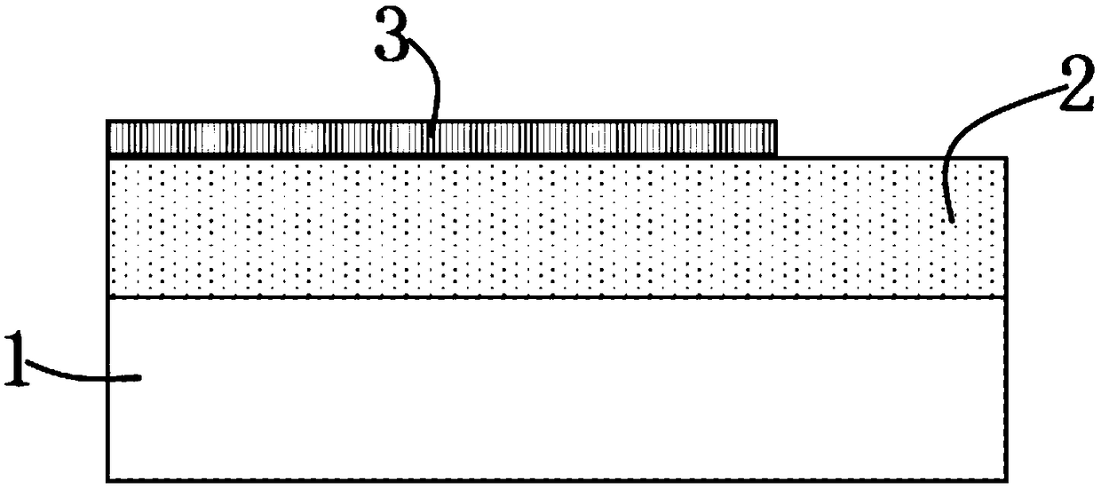
[0055] refer to Figure 2-6 , a thin-film bulk acoustic resonator prepared by the following preparation method:
[0056] Thin film structural layer growth step: depositing (0002) oriented single crystal aluminum nitride layer on the surface of the growth substrate 1 made of silicon which has been cleaned and dried by standard RCA, as the piezoelectric film 2;
[0057] Wherein, the piezoelectric thin film of monocrystalline aluminum nitride layer can be 50sccm (standard state milliliter / min) in trimethylaluminum (TMA) flow rate, NH 3 The flow rate is 3slm (standard state liter / min), the Ar flow rate is 1slm, the substrate temperature is 950°C, the total pressure of the reaction chamber is 40Tor, and it is deposited by MOCVD (metal organic compound chemical vapor deposition) under the parameters;
[0058] Steps for making the top electrode: using a radio frequency magnetron sputtering system, using a pure molybdenum target (purity 99.999%) to sputter deposit a layer of metal mo...
Embodiment 2
[0065] A thin film bulk acoustic resonator prepared by the following preparation method:
[0066] Thin film structure layer growth step: deposit (0002) oriented single crystal aluminum nitride layer on the surface of the growth substrate made of silicon after standard RCA cleaning and drying, as a piezoelectric film;
[0067] Wherein, the piezoelectric thin film of monocrystalline aluminum nitride layer can be 55sccm (standard state milliliter / min) in trimethylaluminum (TMA) flow rate, NH 3 The flow rate is 4slm (liter / min in standard state), the Ar flow rate is 2slm, the substrate temperature is 960°C, the total pressure of the reaction chamber is 45Tor, and it is deposited by MOCVD (metal organic compound chemical vapor deposition) under the parameters;
[0068] Top electrode manufacturing steps: using a radio frequency magnetron sputtering system, use a pure molybdenum target (purity 99.999%) to sputter deposit a layer of metal molybdenum on the surface of the single crysta...
PUM
 Abstract
Description
Claims
Application Information
 - Generate Ideas
- Intellectual Property
- Life Sciences
- Materials
- Tech Scout
- Unparalleled Data Quality
- Higher Quality Content
- 60% Fewer Hallucinations
Browse by: Latest US Patents, China's latest patents, Technical Efficacy Thesaurus, Application Domain, Technology Topic, Popular Technical Reports.
© 2025 PatSnap. All rights reserved.Legal|Privacy policy|Modern Slavery Act Transparency Statement|Sitemap|About US| Contact US: help@patsnap.com


