Femtosecond laser direct writing method of copper antioxidant microstructure and copper ion ink
A technology of femtosecond laser and copper ions, which is applied in the fields of optics, ink, and optomechanical equipment, can solve the problems of cumbersome flexible electrode manufacturing technology, unsatisfactory conductivity of carbon nanomaterials, and high cost of precious metal inks, achieving small thermal effects, The preparation process is simple and the effect of improving conductivity
- Summary
- Abstract
- Description
- Claims
- Application Information
AI Technical Summary
Problems solved by technology
Method used
Image

Examples
preparation example Construction
[0035] (1) Preparation of copper ion ink: the main material components of copper ion ink are copper salt, polyvinylpyrrolidone (PVP), polyethylene glycol (PEG), etc., which are mixed and treated with an ultrasonic cell disruptor.
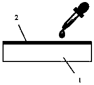
[0036] (2) Preparation of copper ion film: After the substrate to be used is cleaned with organic solvent and soaked in deionized water, copper ion ink is drip-coated or spin-coated on the cleaned substrate, and dried to obtain a copper film with a thickness of 100-500 μm. ion membrane.
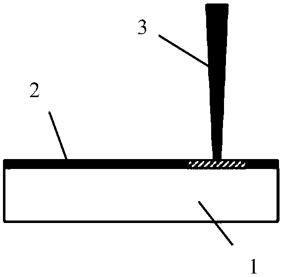
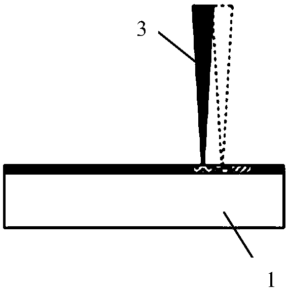
[0037] (3) Femtosecond laser direct writing copper wire: build a femtosecond laser optical path, use femtosecond laser to directly write electrodes on the film, and use a computer-controlled high-precision two-dimensional mobile platform to obtain the expected circuit.
[0038] (4) Removing the area not irradiated by the femtosecond laser: washing the substrate with an organic solvent and water in sequence, and finally obtaining a substrate printed with a circuit. ...
example 1
[0050] Add 0.97g of copper nitrate, 0.1g of polyvinylpyrrolidone (PVP), and 0.2g of polyethylene glycol (PEG) into 10ml of deionized water, treat it with an ultrasonic cell breaker for 15min, and drop-coat it on the cleaned polycarbonate On the resin (PC) plastic substrate, after drying, a film with a thickness of about 150 μm is formed. see Figure 2-4 , using 800nm femtosecond laser 3 for laser direct writing, the laser power is 1W, and the scanning speed is 25μm / s, and finally a conductive copper wire 4 with a resistivity of 1×10⁻⁵Ω·m is obtained. If the laser power is increased to 2.5W and the scanning speed remains unchanged, a conductive copper wire with a resistivity of 1×10⁻³Ω·m can be obtained.
example 2
[0052] Add 1.25g of copper nitrate, 0.1g of polyvinylpyrrolidone (PVP), and 0.2g of polyethylene glycol (PEG) into 10ml of deionized water, treat it with an ultrasonic cell breaker for 15min, and drop-coat it onto the cleaned glass substrate. On the chip, after drying, a film with a thickness of about 230 μm is formed. 800nm femtosecond laser is used for laser direct writing, the laser power is 1W, and the scanning speed is 25μm / s, and finally a conductive copper wire with a resistivity of 5×10⁻⁶Ω·m is obtained.
[0053] In an embodiment, the resistivity of the obtained copper microstructure can be controlled by adjusting parameters such as the repetition frequency, power, and scanning speed of the femtosecond laser, and the width of the copper microstructure can be controlled by adjusting the spot size. The energy of the laser under different parameters With different densities, there will be differences in the amount and connection degree of the reduced copper nanoparticle...
PUM
| Property | Measurement | Unit |
|---|---|---|
| Resistivity | aaaaa | aaaaa |
Abstract
Description
Claims
Application Information
 - R&D
- Intellectual Property
- Life Sciences
- Materials
- Tech Scout
- Unparalleled Data Quality
- Higher Quality Content
- 60% Fewer Hallucinations
Browse by: Latest US Patents, China's latest patents, Technical Efficacy Thesaurus, Application Domain, Technology Topic, Popular Technical Reports.
© 2025 PatSnap. All rights reserved.Legal|Privacy policy|Modern Slavery Act Transparency Statement|Sitemap|About US| Contact US: help@patsnap.com