Eureka AIR delivers breakthrough ideas for toughest innovation challenges, trusted by R&D personnel around the world.

Power device protection chip and preparation method thereof

A technology for protecting chips and power devices, which is applied in the field of power device protection chips and its preparation, can solve problems affecting circuit stability and large circuit signal attenuation, and achieve the effects of reducing manufacturing costs, reducing parasitic capacitance, and reducing conduction loss

Active Publication Date: 2021-06-18
SHENZHEN MYD INFORMATION TECH CO LTD
View PDF4 Cites 0 Cited by
  • Summary
  • Abstract
  • Description
  • Claims
  • Application Information

AI Technical Summary

Problems solved by technology

In high-frequency circuits, because the surge protection chip also has parasitic capacitance, the signal attenuation of the circuit is relatively large, and even the stability of the entire circuit is affected.

Method used


Image

  • Power device protection chip and preparation method thereof
  • Power device protection chip and preparation method thereof
  • Power device protection chip and preparation method thereof

Examples


Embodiment Construction

[0025] In order to understand the specific technical solutions, features and advantages of the present invention more clearly, the present invention will be further described in detail below in conjunction with the accompanying drawings and specific embodiments.

[0026] In the description of the present invention, it should be noted that the terms "upper", "lower", "left", "right", "transverse", "longitudinal", "horizontal", "inner", "outer" etc. indicate The orientation or positional relationship is based on the orientation or positional relationship shown in the drawings, or the orientation or positional relationship that is usually placed when the product of the invention is used, and is only for the convenience of describing the present invention and simplifying the description, rather than indicating or implying the It should not be construed as limiting the invention that a device or element must have a particular orientation, be constructed, and operate in a particular ...


PUM


Abstract

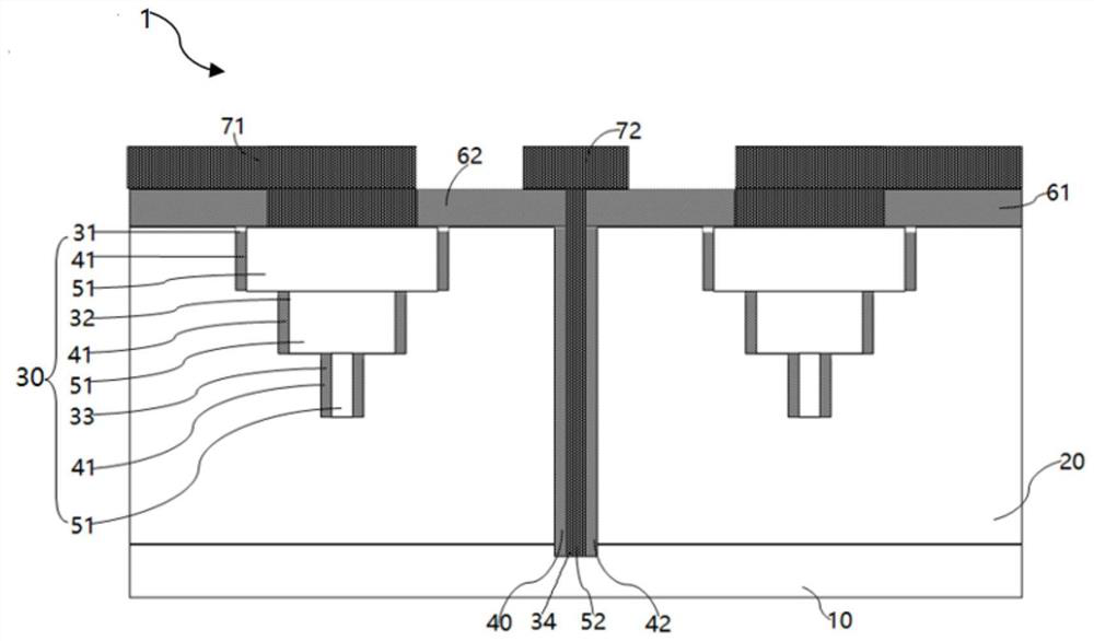
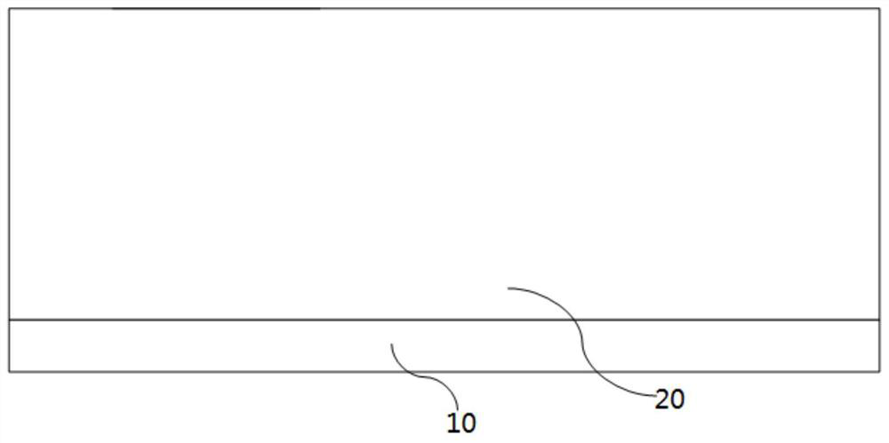
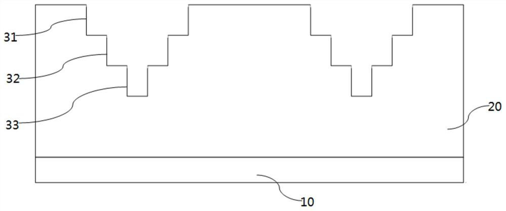
The invention provides a power device protection chip, which includes a substrate; an epitaxial layer formed on the substrate; a rectification region formed in the epitaxial layer at intervals, and the rectification region includes a first groove formed from the upper surface of the epitaxial layer into the epitaxial layer groove, a second groove formed from the bottom of the first groove into the epitaxial layer, and a third groove formed from the bottom of the second groove into the epitaxial layer, the first groove, the second groove and the third The grooves are connected and the widths are successively reduced. The first metal layer is filled in the first groove, the second groove and the third groove, and the first metal layer in the first groove, the second groove and the third groove The height of the Schottky barrier between the epitaxial layer and the epitaxial layer decreases in turn; the isolation region extending from the upper surface of the epitaxial layer to the substrate between the two rectification regions, the isolation region includes the fourth trench and fills the fourth The trench is in ohmic contact with the substrate on the second metal layer. The invention also provides a preparation method for the protection chip of the power device, which enhances the stability, reduces the encapsulation area and reduces the preparation cost.

Description

technical field [0001] The invention relates to the technical field of semiconductor chip manufacturing technology, in particular to a power device protection chip and a preparation method thereof. Background technique [0002] As semiconductor devices become increasingly smaller, denser, and more versatile, electronic devices are increasingly susceptible to voltage surges, which can induce transient current spikes in everything from electrostatic discharge to lightning. Electrostatic discharge (ESD) and other random voltage transients in the form of voltage surges exist in a variety of electronic devices. [0003] Surge protection chip is a solid-state semiconductor device specially designed to protect sensitive semiconductor devices from transient voltage surge damage. It has small clamping coefficient, small size, fast response, small leakage current and reliable High performance, so it has been widely used in voltage transient and surge protection. Based on different a...

Claims


Application Information

Patent Timeline
Patent Type & Authority Patents(China)
IPC IPC(8): H01L27/02H01L29/872H01L21/329
CPCH01L27/0255H01L29/66143H01L29/872
Inventor 不公告发明人
Owner SHENZHEN MYD INFORMATION TECH CO LTD
Why Eureka
Eureka Blog
Learn More