


Quick Research
Generate reliable direction feasibility study reports for your R&D in just a few steps.

Technical Q&A
Discover and master advanced knowledge NOW. Basics, ideas, possibilities, all at once.

Find Solutions
As an expert in R&D theories, this can generate solutions to your technical problems instantly.

Evaluate Feasibility
Analyze your overall solution with one click, know your potential R&D risks in advance.

Monitor Landscape
Get weekly tech updates, stay abreast of the latest tech innovations and key insights.
A GaN based wide swing linearize device and a manufacturing method thereof
A manufacturing method and gallium nitride-based technology, applied in the field of radio frequency, can solve problems such as high cost and complex circuit, and achieve the effect of low cost, simple device structure and widening range
- Summary
- Abstract
- Description
- Claims
- Application Information
AI Technical Summary
Problems solved by technology
Method used
Image

Examples
Embodiment 1
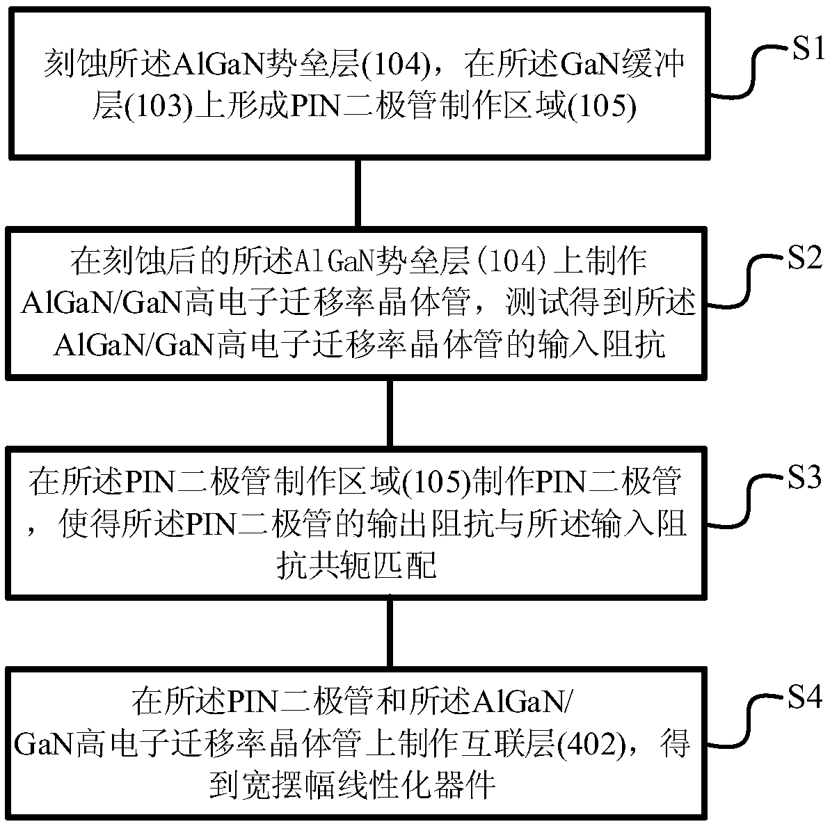
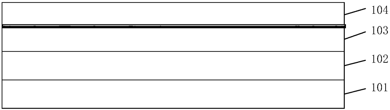
[0044] See figure 1 , figure 1 The flow chart of the fabrication method of the GaN-based wide-swing linearization device provided for the embodiment of the present invention, the AlGaN / GaN high electron mobility transistor includes the first substrate layer 101, the nucleation layer 102, the GaN buffer layer 103 and the AlGaN Fabricated on a sample of the barrier layer 104, see Figure 2a , wherein a two-dimensional electron gas (Two dimensional electrons, 2DEG) exists between the buffer layer 103 and the barrier layer 104 . First, clean the sample. The cleaning steps are as follows: place the sample in acetone for 2 minutes, and then boil it in a positive glue stripping solution heated in a water bath at 60°C for 10 minutes. After washing off residual acetone and ethanol with deionized water, use HF solution (HF: H 2 O=1:5) Clean the sample for 30s, and finally clean it with deionized water and dry it with ultra-pure nitrogen.
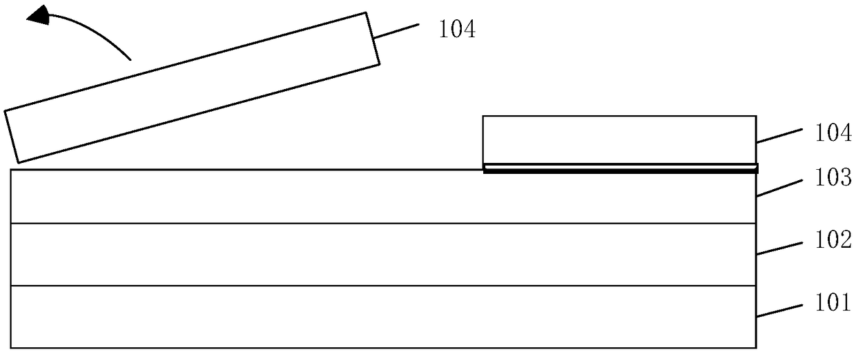
[0045] After cleaning, a PIN diode fabricat...
Embodiment 2
[0081] See Figure 3a-Figure 3f , Figure 3a-Figure 3f It is a schematic diagram of the manufacturing method of the PIN diode provided by the embodiment of the present invention.
[0082] According to the measured input impedance of the AlGaN / GaN HEMT device, the output impedance of the PIN diode is Z d = r 1 +jxΩ, the junction capacitance of the PIN diode can be calculated from the output impedance. From the junction capacitance, it is known that the size and doping concentration of the PIN diode affect its size, thereby affecting the output impedance of the PIN diode. Therefore, by controlling the size and doping concentration of the PIN diode impurity concentration to make PIN diodes.
[0083] The preparation steps of the PIN diode are as follows:
[0084] S31. In the PIN diode fabrication region 105, epitaxially N+ layer material, I layer material, and P+ layer material in sequence to form N+ layer 301, I layer 302, and P+ layer 303 in sequence; please refer to Figur...
Embodiment 3
[0108] See Figure 4a-Figure 4b , Figure 4a-Figure 4b The schematic diagram of the interconnection method of the wide-swing linearization device provided by the embodiment of the present invention, the specific steps are as follows:
[0109] S41. Photolithographically etch the opening area of the interconnection layer on the first protection layer 207 and the second protection layer 307, and etch the first protection layer 207, the dielectric layer 204 and the second protection layer in the opening area of the interconnection layer layer 307, forming an open cell structure 501; see Figure 4a ,Specific steps are as follows:
[0110]S411. Lithographically etched the opening area of the metal interconnection layer in the first protective layer 207 and the second protective layer 307: first, put the sample on a hot plate at 200° C. and bake for 5 minutes; On the protective layer 307, the photoresist is glued and glued, and the speed of glue spinning is 3500r / min, and th...
PUM
 Abstract
Description
Claims
Application Information
 - R&D Engineer
- R&D Manager
- IP Professional
- Industry Leading Data Capabilities
- Powerful AI technology
- Patent DNA Extraction
Browse by: Latest US Patents, China's latest patents, Technical Efficacy Thesaurus, Application Domain, Technology Topic, Popular Technical Reports.
© 2024 PatSnap. All rights reserved.Legal|Privacy policy|Modern Slavery Act Transparency Statement|Sitemap|About US| Contact US: help@patsnap.com