


Quick Research
Generate reliable direction feasibility study reports for your R&D in just a few steps.

Technical Q&A
Discover and master advanced knowledge NOW. Basics, ideas, possibilities, all at once.

Find Solutions
As an expert in R&D theories, this can generate solutions to your technical problems instantly.

Evaluate Feasibility
Analyze your overall solution with one click, know your potential R&D risks in advance.

Monitor Landscape
Get weekly tech updates, stay abreast of the latest tech innovations and key insights.
Metal gallium oxide doping transparent conductive membrane used for ultraviolet waveband and preparation method thereof
A transparent conductive film, ultraviolet band technology, applied to conductive layers on insulating carriers, metal material coating processes, circuits, etc., can solve problems such as low conductivity and poor contact characteristics, and achieve simple preparation methods, reduced resistance, The effect of increasing the difficulty of the process
- Summary
- Abstract
- Description
- Claims
- Application Information
AI Technical Summary
Problems solved by technology
Method used
Image


Examples
Embodiment 1
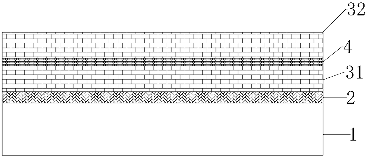
[0034] figure 1 Be a kind of novel metal doping Ga of specific embodiment 2 o 3 Schematic diagram of the cross-section of the film before high-temperature annealing; figure 1 As shown, a method for preparing a metal-doped gallium oxide transparent conductive film for ultraviolet bands comprises the following steps:
[0035] 1) On the substrate 1 cleaned by sulfuric acid, hydrogen peroxide and ammonia respectively in a 60°C water bath, the contact layer film 2 was conventionally grown by electron beams. The contact layer film 2 was made of ITO with a thickness of 10nm. Annealed under atmosphere for 1 min.
[0036] 2) Use magnetron sputtering with 140W power, substrate speed 20rmp, and 5mtorr argon gas to grow the first layer of Ga by sputtering 2 o 3 For the thin film 31, the sputtering time is preferably 10 minutes, and the thickness is 15 nm.
[0037] 3) Using magnetron sputtering with a power of 100W, a substrate speed of 20rmp, and argon gas of 5mtorr to grow the dope...
Embodiment 2
[0048] A method for preparing a metal-doped gallium oxide transparent conductive film for ultraviolet band, comprising the steps of:
[0049] 1) On the substrate 1 cleaned by sulfuric acid, hydrogen peroxide and ammonia respectively in a 60°C water bath, the contact layer film 2 was conventionally grown by electron beams. The contact layer film 2 was made of Ni with a thickness of 4nm. Annealed under atmosphere for 1 min.
[0050] 2) Use magnetron sputtering with 140W power, substrate speed 20rmp, and 5mtorr argon gas to grow the first layer of Ga by sputtering 2 o 3 For the thin film 31, the sputtering time is preferably 10 minutes, and the thickness is 15 nm.
[0051] 3) Using magnetron sputtering with a power of 100W, a substrate speed of 20rmp, and argon gas of 5mtorr to grow the doped film 4 by sputtering, the doped film 4 is an Ag film with a thickness of 7nm;
[0052] 4) Use magnetron sputtering with 140W power, substrate speed 20rmp, and 5mtorr argon gas to grow the...
Embodiment 3
[0056] A method for preparing a metal-doped gallium oxide transparent conductive film for ultraviolet band, comprising the steps of:
[0057] 1) On the substrate 1 cleaned by sulfuric acid, hydrogen peroxide and ammonia respectively in a 60°C water bath, the contact layer film 2 was conventionally grown by electron beams. The contact layer film 2 was made of ITO with a thickness of 10nm. Annealed under atmosphere for 1 min.
[0058] 2) Use magnetron sputtering with 140W power, substrate speed 20rmp, and 5mtorr argon gas to grow the first layer of Ga by sputtering 2 o 3 For the thin film 31, the sputtering time is preferably 10 minutes, and the thickness is 10 nm.
[0059] 3) Using magnetron sputtering with a power of 100W, a substrate speed of 20rmp, and argon gas of 5mtorr to grow the doped film 4 by sputtering, the doped film 4 is an Ag film with a thickness of 7nm;
[0060] 4) Use magnetron sputtering with 140W power, substrate speed 20rmp, and 5mtorr argon gas to grow t...
PUM
| Property | Measurement | Unit |
|---|---|---|
| thickness | aaaaa | aaaaa |
| thickness | aaaaa | aaaaa |
| thickness | aaaaa | aaaaa |
Abstract
Description
Claims
Application Information
 - R&D Engineer
- R&D Manager
- IP Professional
- Industry Leading Data Capabilities
- Powerful AI technology
- Patent DNA Extraction
Browse by: Latest US Patents, China's latest patents, Technical Efficacy Thesaurus, Application Domain, Technology Topic, Popular Technical Reports.
© 2024 PatSnap. All rights reserved.Legal|Privacy policy|Modern Slavery Act Transparency Statement|Sitemap|About US| Contact US: help@patsnap.com