Electrically conductive die bond adhesive applied to packaging large-size chips, method for preparing electrically conductive die bond adhesive and application thereof
A technology of chip packaging and bonding glue, which is applied in the direction of conductive adhesives, electric solid devices, semiconductor/solid device components, etc.
- Summary
- Abstract
- Description
- Claims
- Application Information
AI Technical Summary
Problems solved by technology
Method used
Image

Examples
Embodiment 1
[0036] A method for preparing a conductive die-bonding adhesive applied to large-scale chip packaging, the specific steps are as follows: 8 parts of hydroxyl-terminated polybutadiene acrylonitrile HTBN, 6 parts of thermoplastic resin SG-600TEA, 0.5 part of conductive accelerator 8- Hydroxyquinoline, 4 parts of liquid phenolic resin MEH-8000H are mixed evenly, and then ground twice by a three-roller machine, and then 5 parts of closed latent curing agent SBN-70D are added, mixed evenly, vacuumed for 30 minutes, and 18.75 parts of silver powder SA are added -0201, 18.75 parts of silver powder EA-0001, mix well, vacuum 30min, then add 1.0 parts of coupling agent A-187, mix well, then add the remaining 18.75 parts of silver powder SA-0201, 18.75 parts of silver powder EA-0001, mix Evenly, vacuum for 30min.
[0037] The conductive crystal-bonding adhesive solution is prepared into a roll-shaped film through a coating device.
Embodiment 2
[0039]A method for preparing a conductive die-bonding adhesive applied to large-scale chip packaging, the specific steps are as follows: 2 parts of hydroxyl-terminated polybutadiene acrylonitrile HTBN, 20 parts of thermoplastic resin SG-600TEA, 0.5 parts of conductive accelerator 8- Hydroxyquinoline, 1 part of liquid phenolic resin MEH-8000H, mix well, then grind 2 times through a three-roll machine, then add 10 parts of closed latent curing agent SBN-70D, mix well, vacuum for 30 minutes, add 12.5 parts of silver powder SA-0201, 25.0 parts of silver powder EA-0001, mix well, vacuumize for 30min, then add 1.0 parts of coupling agent A-187, mix well, then add the remaining 12.5 parts of silver powder SA-0201, 25.0 parts of silver powder EA-0001, Mix well and vacuumize for 30min.
[0040] The conductive crystal-bonding adhesive solution is prepared into a roll-shaped film through a coating device.
Embodiment 3
[0042] A method for preparing conductive die-bonding adhesive applied to large-scale chip packaging, the specific steps are as follows: 10 parts of hydroxyl-terminated polybutadiene acrylonitrile HTBN, 5 parts of thermoplastic resin SG-600TEA, 0.5 parts of conductive accelerator 8- Hydroxyquinoline, mix well, then grind 2 times through a three-roller, then add 2 parts of closed latent curing agent SBN-70D, mix well, vacuumize for 30min, add 18.75 parts of silver powder SA-0201, 18.75 parts of silver powder EA- 0001, mix evenly, vacuumize for 30min, then add 0.5 parts of coupling agent A-187, mix well, then add the remaining 18.75 parts of silver powder SA-0201, 18.75 parts of silver powder EA-0001, mix well, vacuumize for 30min.
[0043] The conductive crystal-bonding adhesive solution is prepared into a roll-shaped film through a coating device.
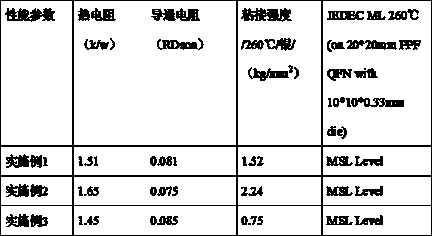
[0044] Table 1 shows the main performance parameters of the conductive adhesive films made from the conductive die-bonding adhesiv...
PUM
 Abstract
Description
Claims
Application Information
 - R&D
- Intellectual Property
- Life Sciences
- Materials
- Tech Scout
- Unparalleled Data Quality
- Higher Quality Content
- 60% Fewer Hallucinations
Browse by: Latest US Patents, China's latest patents, Technical Efficacy Thesaurus, Application Domain, Technology Topic, Popular Technical Reports.
© 2025 PatSnap. All rights reserved.Legal|Privacy policy|Modern Slavery Act Transparency Statement|Sitemap|About US| Contact US: help@patsnap.com