Doped region and IGBT device forming methods, and doped region and IGBT device structures
A technology of device structure and doped region, applied in semiconductor devices, semiconductor/solid-state device manufacturing, electrical components, etc., can solve the problems of increasing edge cell failure rate, edge cell latching effect, large hole current, etc. Achieve the effect of increasing resistance value, strengthening suppression strength and saving cost
- Summary
- Abstract
- Description
- Claims
- Application Information
AI Technical Summary
Problems solved by technology
Method used
Image
Examples
Embodiment 1
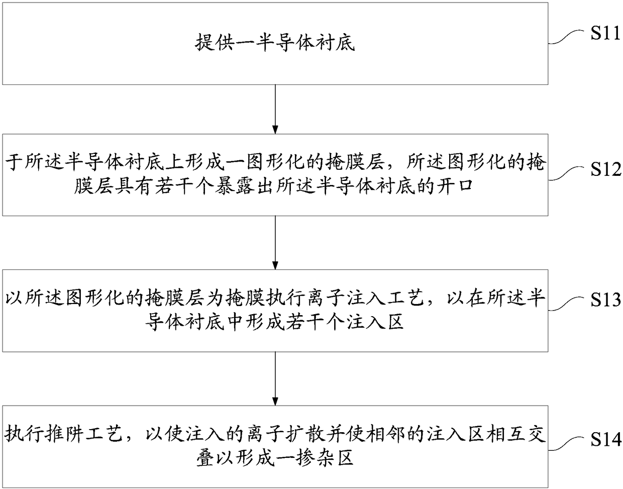
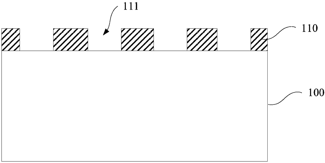
[0056] figure 1 It is a schematic flow chart of the method for forming the doped region in Embodiment 1 of the present invention, Figure 2a - Figure 2d It is a schematic structural diagram during the preparation process of the method for forming the doped region in Embodiment 1 of the present invention. Combine below figure 1 with Figure 2a As shown in -2d, the method for forming the doped region in the embodiment is described in detail.
[0057] First, execute step S11, for details, refer to Figure 2a As shown, a semiconductor substrate 100 is provided. The semiconductor substrate 100 may be an ion-doped semiconductor substrate. In this embodiment, the semiconductor substrate 100 is a semiconductor substrate of the first conductivity type, for example, an N-type semiconductor substrate.
[0058] Next, execute step S12, for details, refer to Figure 2b As shown, a patterned mask layer 110 is formed on the semiconductor substrate 100 , and the patterned mask layer 11...
Embodiment 2
[0063] Based on the method for forming the doped region described above, the present invention also provides a doped region, which is formed by using the method for forming the doped region as described above, that is, the doped region is formed by multiple Two overlapping implanted regions are formed, so that the formed doped regions have a lower doping concentration.
[0064] image 3 It is a schematic diagram of the structure of the doped region in Embodiment 2 of the present invention, such as image 3 As shown, in this embodiment, the doping region 121 is formed in a semiconductor substrate 100, and the doping region 121 includes a plurality of overlapping implantation regions. As mentioned above, since the doped region 121 is formed by overlapping with a plurality of implanted regions after ion diffusion, when forming the doped region 121 with the same area, the doped region 121 in this embodiment lower doping concentration. When the structure of the doped region is f...
Embodiment 3
[0066] Another object of the present invention is to provide a method for forming an IGBT device to form an IGBT device with a transition region. As mentioned above, based on the method for forming the doped region provided by the present invention, it can be applied to the transition region of the IGBT device, so as to effectively improve the effect of concentrating the hole carriers without changing the area of the transition region. the inhibitory strength. At the same time, in the method for forming the IGBT device provided by the present invention, the ion implantation process for forming the doped region is performed simultaneously with the ion implantation processes of other manufacturing processes, which effectively simplifies the process and saves costs. That is, in the method for forming an IGBT device provided by the present invention, while forming the ion implantation process of the confinement ring in the termination region, several implantation regions are als...
PUM
 Abstract
Description
Claims
Application Information
 - Generate Ideas
- Intellectual Property
- Life Sciences
- Materials
- Tech Scout
- Unparalleled Data Quality
- Higher Quality Content
- 60% Fewer Hallucinations
Browse by: Latest US Patents, China's latest patents, Technical Efficacy Thesaurus, Application Domain, Technology Topic, Popular Technical Reports.
© 2025 PatSnap. All rights reserved.Legal|Privacy policy|Modern Slavery Act Transparency Statement|Sitemap|About US| Contact US: help@patsnap.com


