
A new type of infrared detector bib silicon epitaxial wafer manufacturing method

A technology of infrared detectors and manufacturing methods, applied in semiconductor/solid-state device manufacturing, final product manufacturing, sustainable manufacturing/processing, etc., capable of solving problems such as high resistivity

Active Publication Date: 2019-12-27
NANJING GUOSHENG ELECTRONICS
View PDF9 Cites 0 Cited by
  • Summary
  • Abstract
  • Description
  • Claims
  • Application Information

AI Technical Summary

Problems solved by technology

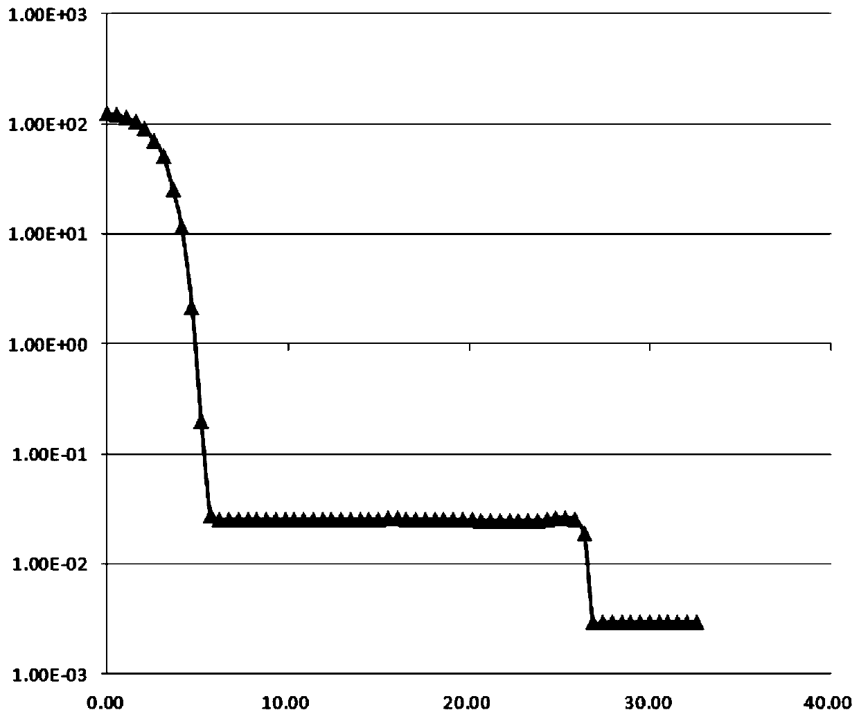
Due to the complexity of silicon epitaxial growth, the resistivity difference between the low-resistance absorbing layer and the intrinsic layer is 5 orders of magnitude, and the interlayer self-doping and cavity environment self-doping have a great influence on the resistivity of the intrinsic layer; and the new BIB infrared detection In order to ensure the accuracy of detection, the detector (blocking impurities with infrared detectors) requires the transition region between the absorption layer and the intrinsic layer to be as wide as possible, and the intrinsic resistivity is as high as possible; the self-doping and intrinsic layer requirements of the high-concentration absorption layer There is a strong conflict between the high resistivity and the narrow transition region, and it is difficult to grow a high-purity barrier layer with a wide flat region on the heavily doped absorber layer

Method used


Image

  • A new type of infrared detector bib silicon epitaxial wafer manufacturing method
  • A new type of infrared detector bib silicon epitaxial wafer manufacturing method
  • A new type of infrared detector bib silicon epitaxial wafer manufacturing method

Examples


Embodiment Construction

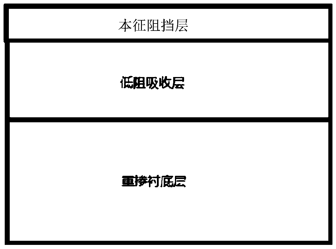
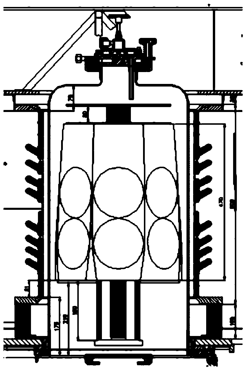
[0020] see figure 1 As shown, the equipment used in the present invention is Italian PE-2061S atmospheric pressure silicon epitaxial growth equipment, the high-purity graphite base is used as a high-frequency induction heating body, and the purity of the main carrier gas H2 is above 99.9999%.

[0021] Equipment preparation includes,

[0022] Reactor cleaning: The quartz bell jar and the quartz parts used in the reaction chamber must be carefully cleaned before epitaxy. The substrate removes the deposition residue on the inner wall of the quartz bell jar and the quartz parts to reduce the self-doping of the cavity.

[0023] High-temperature treatment in the reaction chamber: Before epitaxial growth, the graphite base must be subjected to HCl high-temperature treatment to remove residual reactants adsorbed by the base and cavity, and deposit a layer of intrinsic polysilicon.

[0024] Please reunite image 3 and Figure 4 As shown, the steps of the manufacturing method of the ...


PUM

PropertyMeasurementUnit
electrical resistivityaaaaaaaaaa
thicknessaaaaaaaaaa
thicknessaaaaaaaaaa

Abstract

The present invention relates to a novel infrared detector BIB silicon epitaxial wafer manufacturing method. An N-type (100) polished wafer with heavily doped As, the electrical resistivity is <=0.004[Omega].cm, and there is not a back-seal substrate. In order to reduce the back-face self doping influence, a silicon package process is adapted. Surface impurities and defects are removed through HCI in-situ high-temperature polishing so as to improve the substrate surface quality. Substrate self-doping is reduced through a high-flow high-temperature blowdown process. a two-step extrapolation isemploys to allow a low-resistance absorption layer and an intrinsic layer to be separately grown, and high-flow H2 cooling blowdown between the two steps; and a cavity is subjected to high-flow gas corrosion prior to wafer installation of the epitaxy of the intrinsic layer, the low-speed and low-temperature growth is performed when epitaxy is performed. The novel infrared detector BIB silicon epitaxial wafer manufacturing method controls self-doping, a transition area of the absorption layer and the substrate is steep, the intrinsic barrier layer has a wide flat area so as to meet the demandof the BIB device design.

Description

technical field [0001] The invention belongs to the field of semiconductor basic material silicon epitaxial wafers, and in particular relates to a method for manufacturing a novel infrared detector BIB (impurity band infrared detector) silicon epitaxial wafer. Background technique [0002] Barrier impurity (BIB) detectors have the advantages of wide wavelength coverage, low dark current, high photoconductive gain, fast response, and high radiation resistance. It uses impurity photoconductivity to detect, and because the impurity ionization energy is small, it can respond to longer wave infrared. Traditional extrinsic photoconductive (ESPC) infrared detectors require high doping concentration to improve absorption performance, but their maximum doping concentration is limited by the excessive dark current caused by the resulting impurity band conductance, BIB infrared The detector skillfully introduces an intrinsic layer (blocking layer) between the electrode and the infrare...

Claims


Application Information

Patent Timeline
Patent Type & Authority Patents(China)
IPC IPC(8): H01L31/18H01L21/22
CPCH01L21/2205H01L31/1804Y02P70/50
Inventor 张峰王银海杨帆孙健骆红
Owner NANJING GUOSHENG ELECTRONICS
Learn More