
Tunnel compensating superlattice infrared detector

An infrared detector and superlattice technology, applied in semiconductor devices, electrical components, circuits, etc., can solve the problems of large dark current of devices, widening of quantum wells, narrowing of quantum wells, etc., and achieve fast photoresponse and large Light-responsive, easy-to-make effects

Active Publication Date: 2018-09-14
BEIJING UNIV OF TECH
View PDF4 Cites 0 Cited by
  • Summary
  • Abstract
  • Description
  • Claims
  • Application Information

AI Technical Summary

Problems solved by technology

This kind of detector has the following disadvantages: 1. The size of the photocurrent has nothing to do with the number of quantum wells; 2. When the device is working, there is a compensating recombination current in the conduction band, and the dark current of the device is large.
The specific conditions of the epitaxial structure are difficult to achieve precise control
If the actual doping concentration is lower than the design value, the depletion layer of the tunnel junction will be too wide and the quantum well will be narrowed. If the actual doping concentration is higher than the design value, the depletion layer will be too narrow and the quantum well will become wider, making it difficult to obtain the ideal detection wavelength

Method used


Image

  • Tunnel compensating superlattice infrared detector
  • Tunnel compensating superlattice infrared detector
  • Tunnel compensating superlattice infrared detector

Examples


Embodiment Construction

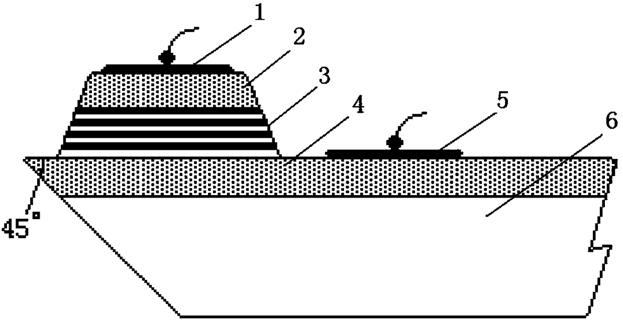
[0026] An infrared detector with tunnel compensation multi-superlattice active regions, in which an N-type lower contact layer 4 is grown on a substrate 6, and then a tunnel compensation superlattice infrared absorption region is grown, and a P-type upper contact layer 2 is grown, and the mesa is made by semiconductor technology , and make an upper metal electrode 1 and a lower metal electrode 5 on the top and bottom of the mesa, the tunnel compensation superlattice infrared absorption region includes a repeating structure formed by at least one basic unit, and the basic unit is a blocking barrier from bottom to top 9. Superlattice infrared absorption region 10, heavily doped N-type region 11 and heavily doped P-type region 12;

[0027] Wherein the heavily doped N-type region 11 and the heavily doped P-type region 12 form a tunnel junction;

[0028] The superlattice infrared absorption region 10 is composed of periodically arranged type I superlattice material systems, and the...


PUM


Abstract

The invention discloses a tunnel compensating superlattice infrared detector, and belongs to the field of semiconductor optoelectronics. The original tunnel compensating multi-active region infrared detector improves the defects that the conventional multiquantum well or superlattice structured infrared detector has small photocurrent and large dark current, yet the original tunnel compensating multi-active region infrared detector is relatively large in production difficulty and low in yield. A lower contact layer is grown on a substrate, then one or more basic units are grown, an upper contact layer is grown, and a table surface and electrodes are produced, wherein the basic units are sequentially a blocking barrier, a superlattice infrared absorption region, a heavily doped N-type region and a heavily doped P-type region; the tunnel compensating superlattice infrared detector is characterized in that a superlattice structure is used as an infrared absorption region of the detector,so that control requirements on epitaxial structural parameters are reduced; the heavily doped N-type region and the heavily doped P-type region form a tunnel junction for providing tunnel compensating current for the superlattice; the blocking barrier has the thickness of 30-50nm so as to reduce the dark current of a device. The tunnel compensating superlattice infrared detector has the advantages of large photocurrent, low dark current, fast response and the like of the tunnel compensating multi-active region infrared detector.

Description

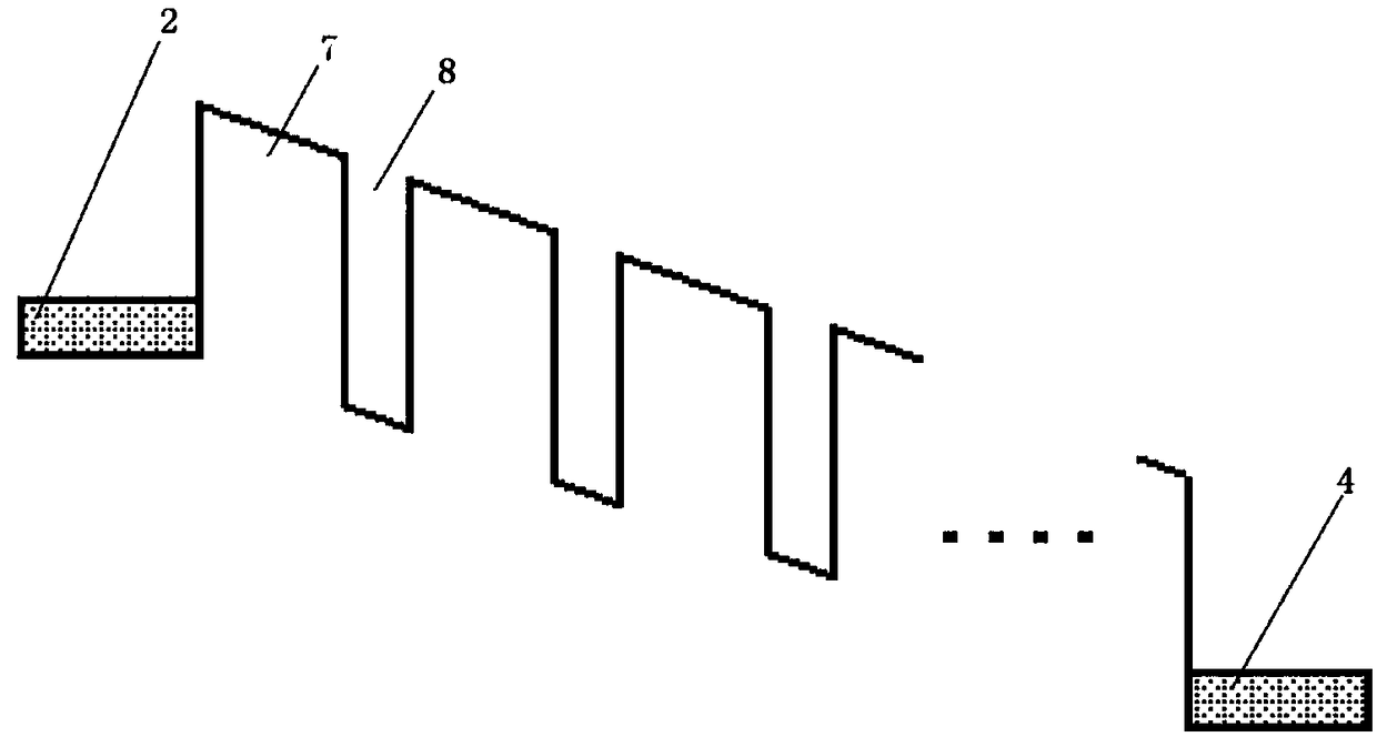
technical field [0001] The invention relates to a medium and long-wavelength infrared detection device, in particular to a tunnel compensation superlattice active region infrared detector, which belongs to the technical field of semiconductor optoelectronics. Background technique [0002] Traditional medium and long wave multiple quantum well or superlattice structure infrared detectors are mainly GaAs / Ga 1-x Al x As material system or In x Ga 1-x As / GaAs material system. The realization of its device structure is obtained by molecular beam epitaxy (MBE) or metal organic chemical vapor deposition (MOCVD or OMVPE) technology epitaxial growth. Through the standard semiconductor process, the traditional medium and long wave multiple quantum well or superlattice structure infrared detection device is obtained, and its basic structure is as follows figure 1 , 2 Shown (in GaAs / Ga 1-x Al x As material system as an example): upper metal electrode 1; upper N-type GaAs contact...

Claims


Application Information

Patent Timeline
Patent Type & Authority Applications(China)
IPC IPC(8): H01L31/0352H01L31/109
CPCH01L31/035236H01L31/035272H01L31/109
Inventor 邓军李超慧徐晨李建军孙伟业韩军
Owner BEIJING UNIV OF TECH
Learn More