A kind of LED epitaxial wafer grown on Si substrate and preparation method thereof

An LED epitaxial wafer and substrate technology, applied in the directions of crystal growth, single crystal growth, chemical instruments and methods, etc., can solve the problems of large tensile stress of the epitaxial layer, cracks of the epitaxial layer, large lattice mismatch, etc. The effect of suppressing lattice mismatch degree and thermal expansion coefficient mismatch, alleviating thermal stress mismatch, and reducing growth temperature

Active Publication Date: 2015-11-11
HEYUAN CHOICORE PHOTOELECTRIC TECH CO LTD
View PDF3 Cites 0 Cited by
  • Summary
  • Abstract
  • Description
  • Claims
  • Application Information

AI Technical Summary

Problems solved by technology

However, although Si has many advantages, the quality of GaN single crystal thin films prepared on Si substrates is not as good as that of sapphire substrates, and there are still many difficulties in the preparation of device-level Si-based LEDs.
First, the lattice mismatch between Si and GaN is still large (about 16%), comparable to that of sapphire, and the defects in GaN epitaxial layers grown on Si are not reduced by orders of magnitude
Secondly, the coefficient of thermal expansion of Si is 2.61×10 -6 / K, the thermal mismatch with GaN is as high as 114%, which is much higher than that of sapphire (about -25.5%), which will cause huge tensile stress in the epitaxial layer, which will more easily cause cracks in the epitaxial layer
Again, when GaN is epitaxially grown on a Si substrate, N 2 Gas, due to the large bond energy of Si-N, when Si substrate meets active N, it is easy to form amorphous Si at the interface. x N y layer, which seriously affects the quality of the obtained GaN-based LED devices

Method used


Image

  • A kind of LED epitaxial wafer grown on Si substrate and preparation method thereof
  • A kind of LED epitaxial wafer grown on Si substrate and preparation method thereof
  • A kind of LED epitaxial wafer grown on Si substrate and preparation method thereof

Examples


Embodiment 1

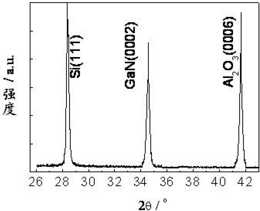
[0033] Please refer to figure 1 , the present invention grows on the LED epitaxial wafer on Si substrate, and it comprises Si substrate layer 11, the Al that grows on Si substrate layer 11 2 o 3 protective layer 12, in Al 2 o 3 A u-GaN buffer layer 13 , an n-GaN layer 14 , an InGaN / GaN quantum well layer 15 and a p-GaN layer 16 are sequentially grown on the protection layer 12 .

[0034] In a preferred scheme, the Al 2 o 3 The thickness of the protection layer 12 is 3-5 nm.

[0035] In a preferred solution, the u-GaN buffer layer 13 includes a low-temperature u-GaN buffer layer and a high-temperature u-GaN buffer layer, and the low-temperature u-GaN buffer layer is grown at a Si substrate temperature of 600-700°C, The high-temperature u-GaN buffer layer is grown under the condition that the Si substrate temperature is 750-850°C.

[0036] The preparation method of the above-mentioned LED epitaxial wafer grown on the Si substrate is as follows:

[0037] Using Si substrat...

Embodiment 2

[0045] This embodiment is improved on the basis of embodiment 1, the difference is: in Al 2 o 3 Before the growth of the protective layer, the pretreatment steps of surface polishing, cleaning, and annealing are performed on the Si substrate in sequence. The specific process is as follows:

[0046] Surface polishing treatment: the surface of the Si substrate is polished with diamond slurry, and no scratches are observed on the surface of the substrate with an optical microscope, and then the substrate is polished by a chemical mechanical polishing method in the prior art.

[0047] Cleaning: put the slot containing the Si substrate into a clean square bottle, add deionized water and prepared acetone until the solution is completely submerged in the Si substrate, and ultrasonicate for 5-10 minutes; put the square bottle into the ultrasonic In the tank, add deionized water until the liquid level of the water is slightly lower than the square bottle, and perform ultrasonic cleani...


PUM

PropertyMeasurementUnit
thicknessaaaaaaaaaa
wavelengthaaaaaaaaaa
full width at half maximumaaaaaaaaaa

Abstract

The invention discloses a light-emitting diode (LED) epitaxial wafer developed on a silicon (Si) substrate. The LED epitaxial wafer developed on the Si substrate is characterized by comprising a Si substrate layer and an aluminum oxide (Al2O3) protective layer developed on the Si substrate layer. A U-GaN buffer layer, an n-GaN layer, an InGaN / GaN quantum well layer and a p-GaN layer are developed on the Al2O3 protective layer. The invention further discloses a preparation method of the LED epitaxial wafer. Compared with the prior art, the LED expitaxial wafer developed on the Si substrate has the advantages of being good in electricity and optical properties, high in crystalline quality and low in defect concentration.

Description

technical field [0001] The invention relates to an LED epitaxial wafer, in particular to an LED epitaxial wafer grown on a Si substrate and a preparation method thereof. Background technique [0002] GaN semiconductor materials have excellent photoelectric properties. Since I.Akasaki successfully obtained p-GaN for the first time and achieved a new breakthrough in blue LEDs, GaN-based compound semiconductors have been attracting attention, and have a wide range of applications in the fields of indoor lighting, commercial lighting, and engineering lighting. Applications. [0003] High-quality GaN materials are generally produced by heteroepitaxial methods. The choice of the substrate has a great influence on the quality of epitaxially grown GaN materials, and generally needs to follow the principles of lattice constant matching, thermal expansion coefficient matching, and affordable price. In addition, different substrate materials also have a very important impact on the f...

Claims


Application Information

Patent Timeline
Patent Type & Authority Patents(China)
IPC IPC(8): H01L33/12H01L33/02H01L33/00C30B25/02C30B25/18
Inventor 李国强
Owner HEYUAN CHOICORE PHOTOELECTRIC TECH CO LTD
Why Eureka
Try Eureka