Laser electrochemical compound micromachining method and device for semiconductor material
A semiconductor and electrochemical technology, applied in the field of laser-electrochemical composite micromachining of semiconductor materials and devices, can solve the problem of unchecked technical literature, etc., to eliminate the recast layer and residual stress, reduce thermal damage, and achieve high processing efficiency. Effect
- Summary
- Abstract
- Description
- Claims
- Application Information
AI Technical Summary
Problems solved by technology
Method used
Image
Examples
Embodiment 1
[0033] Embodiment 1: This embodiment is a semiconductor material laser electrolytic composite processing method based on a localized conductive channel. The laser beam 2 generated by the laser 1 is adjusted and transmitted by an external optical path and then focused on the surface of the semiconductor material 10, and the thermal effect of the laser is used to process high-efficiency materials. Removal, complete micro-hole, micro-groove processing. At the same time, the thermal effect of the laser generates a local temperature field around the microholes, which locally enhances the conductivity of semiconductor materials such as single crystal silicon. On this basis, the stable low-voltage electrolyte beam generation and adjustment device is used to introduce a biased electrolyte beam, and in the region where the conductivity is enhanced around the laser irradiation area, electrochemical anodic dissolution is introduced locally, which can effectively eliminate the recast layer...
Embodiment 2
[0035] Embodiment 2: in combination with figure 1 , the present embodiment is a semiconductor material laser electrolytic composite processing system based on a localized conductive channel, including an optical path system, a stable low-pressure jet generation and adjustment system, and an electrolytic processing system; the optical path system includes a laser 1 and an external optical path, wherein the external optical path includes an optical gate 3. Beam expander 4, vibrating mirror 5 and mirror 6. The laser 1 outputs the laser beam 2, passes through the shutter 3 of the protection device, expands the diameter of the laser beam by the beam expander 4, adjusts the direction through the reflector 6, and finally controls the movement form of the beam by the vibrating mirror 5, irradiates the surface of the semiconductor material 10, and A localized conductive channel 15 is formed within the semiconductor material 10 . Both the generation of the laser beam 2 and the movement...
Embodiment 3
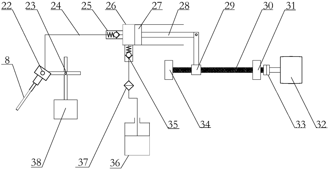
[0040] Embodiment 3: in combination with figure 2 , the embodiment is a stable low-pressure jet flow generation and adjustment system, including a servo motor 32 driving a ball screw 30 to rotate through a coupling 33, and the two ends of the ball screw 30 are supported by the first support seat 32 and the second support seat 35; The slider 29 matched with the ball screw 30 converts the rotation of the ball screw 30 into the linear motion of the piston rod 28 , thereby pushing the electrolyte in the electrolyte cylinder 26 to output at a constant speed. The electrolyte flows into the metal needle 8 through the first one-way valve 25 and the hose 24 to form a stable low-pressure jet. The angle of the low-pressure jet can be adjusted by the angle regulator 22 , and the impact position of the jet can be adjusted by the XYZ three-way fine-tuning platform 38 . The first one-way valve 25 and the second one-way valve 35 can cooperate with the forward and reverse movement of the bal...
PUM
| Property | Measurement | Unit |
|---|---|---|
| electrical conductivity | aaaaa | aaaaa |
| electrical conductivity | aaaaa | aaaaa |
Abstract
Description
Claims
Application Information
 - R&D Engineer
- R&D Manager
- IP Professional
- Industry Leading Data Capabilities
- Powerful AI technology
- Patent DNA Extraction
Browse by: Latest US Patents, China's latest patents, Technical Efficacy Thesaurus, Application Domain, Technology Topic, Popular Technical Reports.
© 2024 PatSnap. All rights reserved.Legal|Privacy policy|Modern Slavery Act Transparency Statement|Sitemap|About US| Contact US: help@patsnap.com


