
Test method for single event effect of germanium-silicon heterojunction transistor based on heavy ion microbeam irradiation

A heterojunction transistor and single-event effect technology, applied in the field of microelectronics, can solve the problems that the physical mechanism of the single-event effect cannot be accurately characterized, and the location of sensitive areas is difficult to achieve by heavy ion broad beam irradiation, so as to achieve effective measurement, reduce The effect of testing cost and improving experimental accuracy

Active Publication Date: 2019-03-26
XIDIAN UNIV
View PDF10 Cites 0 Cited by
  • Summary
  • Abstract
  • Description
  • Claims
  • Application Information

AI Technical Summary

Problems solved by technology

However, for a single transistor device, the overall size of the device is on the order of microns, and it is difficult to locate the sensitive area by heavy ion wide beam irradiation
On the other hand, although the irradiation beam spot of the laser microbeam can achieve a focus size of 1-2 μm, the mechanism of the single event effect induced by the laser is different from that of the heavy ion, and the test results cannot accurately characterize the physical mechanism of the single event effect

Method used


Image

  • Test method for single event effect of germanium-silicon heterojunction transistor based on heavy ion microbeam irradiation
  • Test method for single event effect of germanium-silicon heterojunction transistor based on heavy ion microbeam irradiation
  • Test method for single event effect of germanium-silicon heterojunction transistor based on heavy ion microbeam irradiation

Examples


Embodiment Construction

[0033] Below in conjunction with accompanying drawing and specific embodiment the present invention is described in further detail:

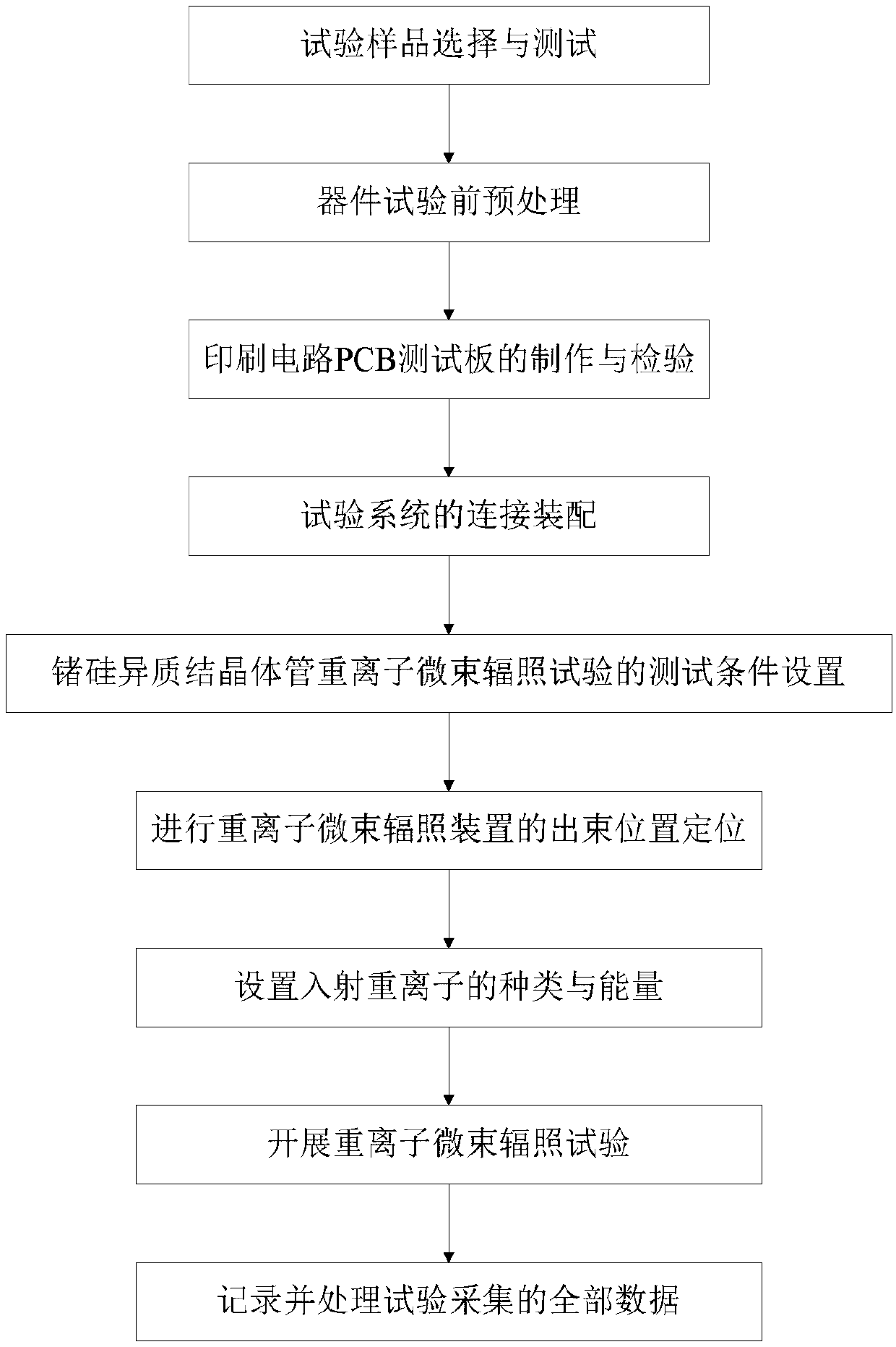
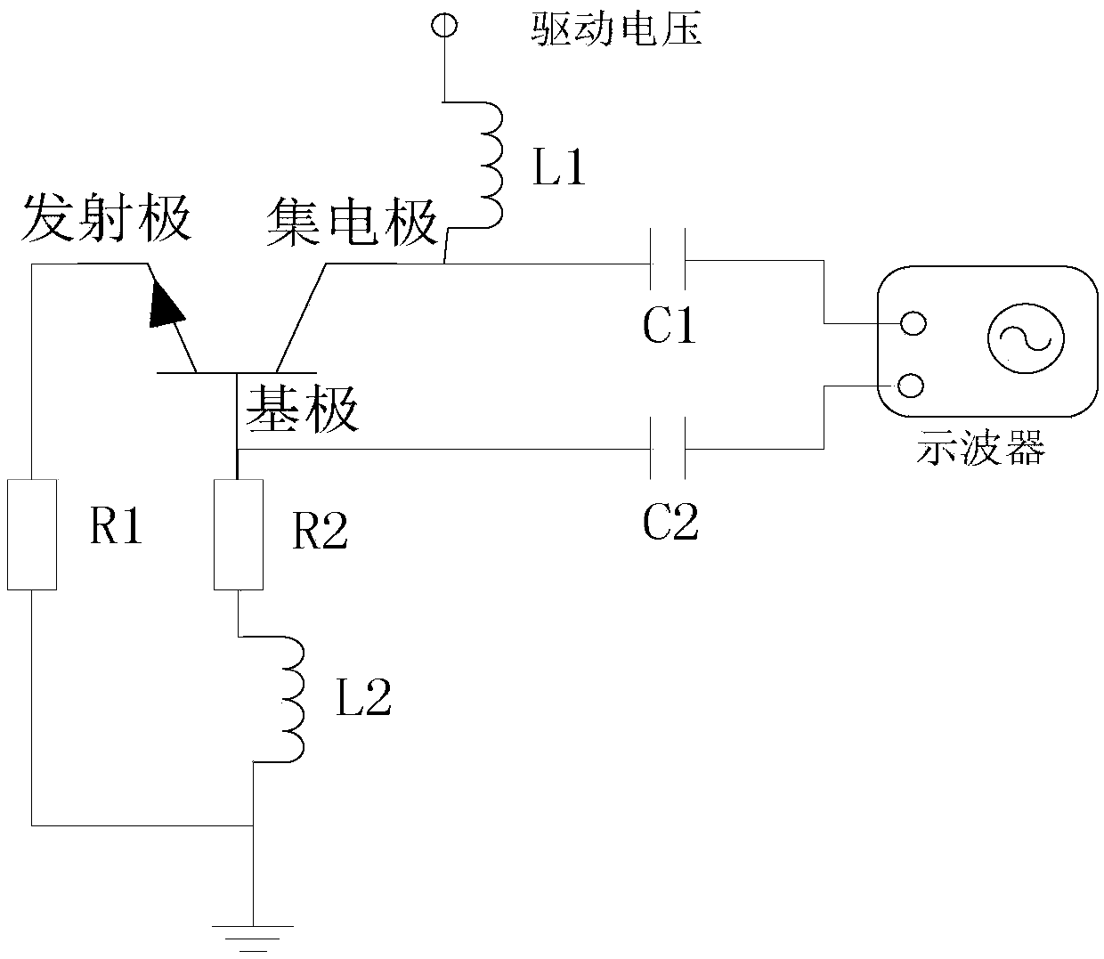
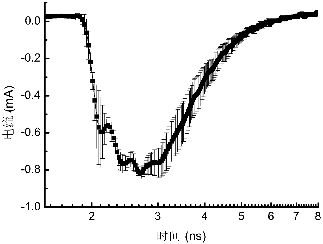
[0034] refer to figure 1 , the present invention is aimed at the heavy ion micro-beam test method of the single event effect of germanium-silicon heterojunction transistors, and its realization steps include the following:

[0035] Step 1, select a silicon-germanium heterojunction transistor sample for the test, and carry out the electrical performance test of the device.

[0036] According to the device manual of the selected silicon-germanium heterojunction transistor, the current amplification factor, open-circuit reverse current, open-circuit breakdown voltage, cut-off frequency and equivalent capacitance of the transistor are selected as test parameters, and the semiconductor parameter tester is used to test the silicon-germanium heterojunction transistor. The junction transistors were tested; considering the certain damage rate in the de-...


PUM


Abstract

The present invention provides a germanium-silicon heterojunction transistor single event effect test method based on heavy ion microbeam irradiation. The problems are mainly solved that a damaging mechanism cannot be directly represented and a sensitive region cannot be accurately located in the prior art. The implementation scheme of the method comprises the steps of: selecting a germanium-silicon heterojunction transistor sample to test electrical properties of the germanium-silicon heterojunction transistor sample; making and testing a PCB test board for irradiation, and performing de-encapsulation processing of a germanium-silicon heterojunction transistor device prior to test; assembling an irradiation platform; setting a test condition of a heavy ion microbeam irradiation test; performing beam ejecting position location of a heavy ion microbeam irradiation device; setting the type and the weight of incident heavy ions; developing the heavy ion microbeam irradiation test; and recoding and processing all the test data, and obtaining a single event effect sensitive region. The method provided by the invention can accurately locate the germanium-silicon heterojunction transistorsingle event effect sensitive region, can improve the experiment precision, can reduce the test cost and can be used for assessment of the astronavigation anti-radiation capacity for microelectronicdevices.

Description

technical field [0001] The invention belongs to the technical field of microelectronics, and in particular relates to a single-event effect test method of a germanium-silicon heterojunction transistor, which can be used for evaluating the anti-radiation capability of spaceflight for microelectronic devices. Background technique [0002] With the rapid development of aerospace technology, the demand for space exploration, search for extraterrestrial energy, and expansion of living space is increasing. Long-term missions such as deep space exploration, space laboratories, and satellite navigation have become the core technologies of the current aerospace field. This puts higher demands on microelectronic devices used in electronic systems for long-term flight. [0003] The working state, reliability and lifespan of an electronic system working in a space environment will be affected by severe high-energy particle radiation and extreme temperature, which may lead to system fail...

Claims


Application Information

Patent Timeline
Patent Type & Authority Patents(China)
IPC IPC(8): G01R31/26
CPCG01R31/2637
Inventor 张晋新郭红霞张凤祁王辉张玲霞吴宪祥冯娟贺王鹏安陆
Owner XIDIAN UNIV
Learn More