
High-voltage IGBT device with a built-in ballast resistor

A ballast resistor and device technology, applied in the field of power semiconductor devices, can solve the problems of inability to effectively limit the short-circuit saturation current, difficult process implementation, and poor compatibility, and achieves improved short-circuit capability of devices, strong process compatibility, and improved The effect of thermal stability

Active Publication Date: 2018-06-15
UNIV OF ELECTRONICS SCI & TECH OF CHINA
View PDF6 Cites 1 Cited by
  • Summary
  • Abstract
  • Description
  • Claims
  • Application Information

AI Technical Summary

Problems solved by technology

For IGBT devices with traditional EBR structure, the emitter ballast resistance consists of a strip N + emitter constitutes because N + The doping concentration in the emitter region is high, and the mobility is mainly dominated by the scattering of ionized impurities. The resistance usually exhibits a negative temperature coefficient, that is, the emitter ballast resistance decreases as the temperature increases; under low temperature and low current conditions, EBR A large resistance value will increase the conduction loss of the IGBT power device. Under the condition of high temperature and high current after a short circuit, the resistance value of the EBR becomes smaller, which cannot effectively limit the short circuit saturation current, and the short circuit capacity will continue to increase as the temperature rises. Weakened; therefore, an IGBT device with an EBR structure with a positive temperature coefficient can effectively improve the short-circuit capability of the device
The prior art scheme shows that ballast resistors with positive temperature coefficients can be used at N + It is realized by introducing nickel-iron alloy or deep-level acceptor impurities into the emission area, but the technical scheme is difficult to realize, and it is not compatible with the traditional manufacturing process, and its resistance manufacturing process itself has high-temperature reliability problems

Method used


Image

  • High-voltage IGBT device with a built-in ballast resistor
  • High-voltage IGBT device with a built-in ballast resistor
  • High-voltage IGBT device with a built-in ballast resistor

Examples


Embodiment Construction

[0023] Embodiments of the present invention are described below through specific examples, and those skilled in the art can easily understand other advantages and effects of the present invention from the content described in this specification. The present invention can also be implemented or applied through other different specific implementation modes, and various modifications or changes can be made to the details in this specification based on different viewpoints and applications without departing from the spirit of the present invention.

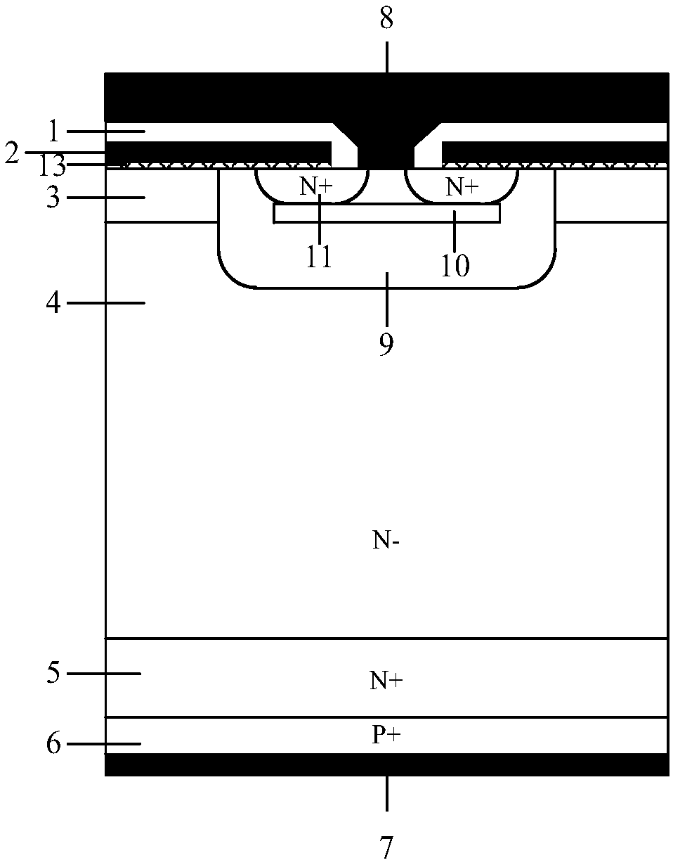
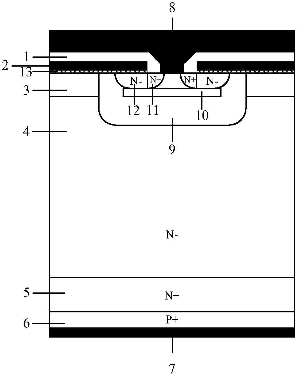
[0024] A high-voltage IGBT device with a built-in ballast resistor, the cell structure of which includes a first conductivity type semiconductor P + Collector region 6, located in the first conductivity type semiconductor P + The metal collector 7 on the back of the collector region 6, the first conductivity type semiconductor P + The second conductive type semiconductor buffer layer 5 above the collector region 6, the second conduct...


PUM


Abstract

The invention provides a high-voltage IGBT device with a built-in ballast resistor. A cell structure includes a first conductivity type semiconductor P+ collector region, a metal collector, a second conductivity type semiconductor buffer layer, a second conductivity type semiconductor N-drift region, a first conductivity type semiconductor P type base region, a heavily doped first conductivity type semiconductor P+ doping region, a second conductivity type semiconductor built-in ballast resistance region, and a heavily doped second conductivity type semiconductor N+ emitter region. The secondconductivity type semiconductor built-in ballast resistance region is used for replacing the part, extending horizontally towards the space below the gate structure, of the second conductivity type semiconductor N+ emitter region, so that the second conductivity type semiconductor built-in ballast resistance region is located in the gate voltage control region. On the basis of the positive temperature characteristic of the ballast resistance value at a high temperature, the short-circuit capability of the device is improved; and the thermal stability of the device in the forward blocking stateis enhanced.

Description

technical field [0001] The invention belongs to the technical field of power semiconductor devices, in particular to a high-voltage IGBT (Insulated Gate Bipolar Transistor) device with a built-in ballast resistor. Background technique [0002] Insulated gate bipolar transistor (Insulated Gate Bipolar Transistor, IGBT) has the advantages of high input impedance of MOSFET, simple driving circuit, and fast switching speed, and has the advantages of high current density and low saturation voltage of bipolar transistors. One of the mainstream power switching devices in the electronic field; it is widely used in high voltage and high current fields, such as wind power generation, rail transit, smart grid, etc. In practical applications, the IGBT will encounter a short-circuit of the load. At this time, the IGBT is subjected to the test of high voltage and high current at the same time. In a short period of time, the chip temperature rises sharply and the heat accumulates, eventual...

Claims


Application Information

Patent Timeline
Patent Type & Authority Applications(China)
IPC IPC(8): H01L29/06H01L29/739
CPCH01L29/0684H01L29/7398
Inventor 李泽宏彭鑫吴玉舟殷鹏飞任敏高巍张金平张波
Owner UNIV OF ELECTRONICS SCI & TECH OF CHINA
Learn More