
Method for auxiliary etching conical array silicon surface through pine structure porous copper

A porous copper and silicon surface technology, applied in sustainable manufacturing/processing, climate sustainability, semiconductor devices, etc., can solve the problem of reducing contact area and hydrophobic performance, large top area, which is not conducive to increasing the amount of light and silicon The ability to receive light and other issues, to achieve the effect of excellent hydrophobic properties and the ability to receive light

Inactive Publication Date: 2018-06-08
NANJING UNIV OF SCI & TECH
View PDF4 Cites 1 Cited by
  • Summary
  • Abstract
  • Description
  • Claims
  • Application Information

AI Technical Summary

Problems solved by technology

Although the columnar array can improve the hydrophobic performance and the ability to receive light on the silicon surface, the top area of ​​the column is still relatively large, which is not conducive to reducing the contact area with water and further improving the hydrophobic performance, which is also not conducive to increasing the irradiation into the array. Further improvement in the amount of light and silicon's ability to receive light

Method used


Image

  • Method for auxiliary etching conical array silicon surface through pine structure porous copper
  • Method for auxiliary etching conical array silicon surface through pine structure porous copper
  • Method for auxiliary etching conical array silicon surface through pine structure porous copper

Examples


Embodiment 1

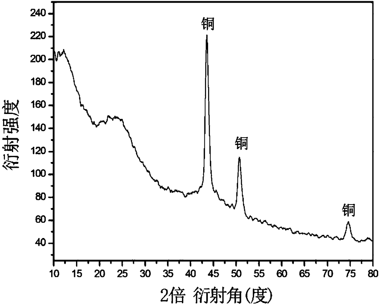
[0036] The white pine wood was placed in an argon-protected sintering furnace and heated to 800 °C at a heating rate of 2 °C / min to obtain a porous carbon with a white pine wood structure; Immersed in the medium for 2 hours, then took out and dried after immersion; the dried porous carbon was sintered to 500 °C in an argon-protected heating furnace to obtain porous copper with a white pine structure; figure 1 Shown is the scanning electron micrograph of the microstructure of the prepared porous copper. It can be seen that the microstructure of the white pine wood is well preserved by the porous copper. figure 2 Shown is the X-ray diffraction pattern of the prepared porous copper, and the material is copper from the diffraction peaks. Prepare a mixed liquid etchant of hydrofluoric acid, hydrogen peroxide, and water. The volume ratio of hydrofluoric acid, hydrogen peroxide, and water is 6:2:2, and immerse the monocrystalline silicon with the etchant. At this time, no corrosion ...

Embodiment 2

[0038] The white pine wood was placed in an argon-protected sintering furnace and heated to 800 °C at a heating rate of 2 °C / min to obtain a porous carbon with a white pine wood structure; After immersion in the carbon for 2 hours, take it out and dry it; the dried porous carbon is sintered to 500 ℃ in an argon-protected heating furnace to obtain porous copper with a white pine structure. Prepare a mixed liquid etchant of hydrofluoric acid, hydrogen peroxide, and water, the volume ratio of hydrofluoric acid, hydrogen peroxide, and water is 6:2:2, and immerse the monocrystalline silicon with the etchant. Press the porous copper on the silicon plane to make it fully contact, so as to play a catalytic role and cause the corrosion reaction to occur. The contact time is 41 minutes, and the silicon-based surface of the cone-shaped array is obtained.

Embodiment 3

[0040] The white pine wood was placed in an argon-protected sintering furnace and heated to 500 °C at a heating rate of 1 °C / min to obtain a porous carbon with a white pine wood structure; Immersed in the carbon for 3 hours, took out and dried after immersion; the dried porous carbon was sintered to 500 °C in an argon-protected heating furnace to obtain porous copper with a white wood structure. Prepare a mixed liquid etchant of hydrofluoric acid, hydrogen peroxide, and water, the volume ratio of hydrofluoric acid, hydrogen peroxide, and water is 6:2:2, and immerse the monocrystalline silicon with the etchant. Press the porous copper on the silicon plane to make it fully contact, so as to play a catalytic role and cause the corrosion reaction to occur. The contact time is 39 minutes, and the silicon-based surface of the cone-shaped array is obtained.

[0041] The porous copper with pine structure used in the present invention is different from other metal catalysts (such as po...


PUM


Abstract

The invention discloses a method for auxiliary etching the conical array silicon surface through pine structure porous copper. Firstly the pine wood is sintered in the non-oxidizing atmosphere to obtain porous carbon having a pine structure, then the porous carbon is immersed in a copper nitrate solution, and porous copper having the pine structure is obtained after drying and anaerobic sintering;and the porous copper acts as the catalyst and is put on the silicon plane, monocrystalline silicon is immersed in a corrosive, and the silicon surface is corroded under the catalytic auxiliary effect of the copper so as to form the conical array silicon surface having the opposite convex-concave structure of that of the porous copper. According to the manufactured silicon surface conical array structure, the microscopic structure of the pine is topological, high degree of learning from the nature is realized and the excellent hydrophobicity and the photon receiving capacity can be acquired;and the acquired conical array silicon surface has the advantages of further narrow top part and smaller contact area with the water so that the adhesion of the silicon surface to the water can be further reduced and the better hydrophobicity can be acquired.

Description

technical field [0001] The invention belongs to a method for preparing a silicon-based hydrophobic and anti-reflection surface, in particular to a method for assisting etching of a cone-shaped array silicon surface by using pine-structured porous copper. Background technique [0002] As an important semiconductor material, silicon has special properties in optics, electricity, magnetism and heat, and is widely used in electronic materials of various semiconductor devices and integrated circuits. If these electronic devices are exposed to the air, it is very easy to absorb dust, or adhere to water vapor, which will cause a short circuit in the circuit and cause the electronic device to fail. Therefore, the preparation of a silicon-based surface hydrophobic structure helps to protect the circuit and achieve self-cleaning of the surface of electronic devices. Especially for devices used outdoors, such as solar panels, which are exposed to the external environment for a long ti...

Claims


Application Information

Patent Timeline
Patent Type & Authority Applications(China)
IPC IPC(8): H01L31/0216H01L31/18
CPCH01L31/02167H01L31/02168Y02P70/50
Inventor 王天驰陈凯冯成黄一轩孔诚谭涵菲
Owner NANJING UNIV OF SCI & TECH
Learn More