Light source component

A technology of components and light sources, applied in the field of semiconductor optoelectronics, can solve the problems of affecting the working junction temperature of the chip, reducing the thermal conductivity of the chip, affecting the heat dissipation of the chip, etc., to improve the welding qualification rate, improve the stability, and ensure the effect of welding yield

Active Publication Date: 2018-05-29
YANGZHOU UNIV
View PDF6 Cites 9 Cited by
  • Summary
  • Abstract
  • Description
  • Claims
  • Application Information

AI Technical Summary

Problems solved by technology

Too much solder will cause the solder to overflow each other and form a short circuit; too little solder will reduce the heat conduction surface of the chip and affect the working junction temperature of the chip; under normal circumstances, the packaging process will prevent factors such as virtual soldering, and the amount of solder paste will exceed the chip electrodes. And it is necessary to form a wide isolation Gap between the positive and negative electrodes of the substrate to ensure that the electrodes are not short-circuited, thereby sacrificing the heat conduction area of ​​the chip, especially when small chips are soldered, the fixed GAP width design occupies a larger total chip area , which seriously affects the heat dissipation when the chip is in use

Method used


Image

  • Light source component
  • Light source component
  • Light source component

Examples


Embodiment Construction

[0024] Embodiments of the present invention will be described in further detail below in conjunction with the accompanying drawings.

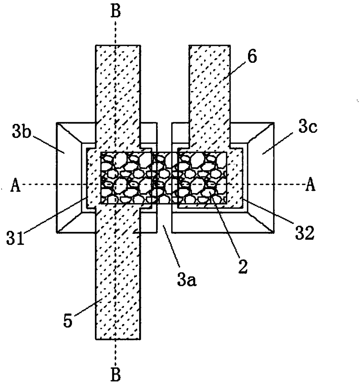
[0025] The reference signs are: substrate body 1, LED chip 2, N electrode 21, P electrode 22, insulating wall 23, mounting boss 3, isolation groove 3a, negative conduction slope 3b, positive conduction slope 3c, negative electrode Area 31 , positive electrode area 32 , thermally conductive insulating layer 4 , negative electrode lead 5 , positive electrode lead 6 , solder 7 .

[0026] The invention discloses a light source element which has strong heat dissipation capability and can prevent electric leakage failure caused by mutual overflow of solder, and improve the qualified rate of product production. The light source element includes a substrate body 1 and a plurality of LEDs welded on the substrate body 1 by solder The chip 2 and the substrate body 1 have good thermal conductivity to facilitate heat dissipation. The best material of the su...


PUM


Abstract

The invention discloses a light source component, which comprises a substrate body and an LED chip, wherein an electrode surface of the LED chip faces the substrate body and comprises an N electrode and a P electrode; a plurality of mounting blocks for arranging the LED chip in a welding manner are formed on the substrate body; each mounting block is a mounting boss which protrudes above a board of the substrate body; a heat-conducting insulating layer covers the substrate body and the surfaces of the mounting blocks; each mounting boss is partitioned into a negative electrode area and a positive electrode area through an isolation groove; a negative electrode lead and a positive electrode lead are printed on the heat-conducting insulating layer; the LED chip is provided with an insulatingwall between the N electrode and the P electrode; and the lower end surface of the insulating wall is laminated with the upper surface of the heat-conducting insulating layer in the isolation grooves. According to the light source component, the welding yield of the LED chip in a relatively small GAP can be ensured, the heat dissipation capability of the component is improved, the stability of the welding process of the LED chip is improved, a short-circuit failure risk caused by mutual overflow infiltration of solder is avoided and the mass production requirements of a high-brightness and high-heat-dissipation light-emitting component can be met.

Description

technical field [0001] The invention belongs to the field of semiconductor optoelectronics, and relates to a semiconductor light-emitting device, in particular to a light source element. Background technique [0002] With the continuous development of the LED light-emitting diode industry and the continuous improvement of technology, the amount of light obtained by the semiconductor element per unit area is getting higher and higher, and the chip size is getting smaller and smaller. Reliability also puts forward higher requirements. Flip-chip is based on the characteristics of its different sides of light emission and heat dissipation. It can make good use of its flip-chip welding and other processes to make the device heat transfer from the electrode surface to the heat sink faster, ensuring that the LED chip can also be used under high current density injection. Maintain good luminous efficiency. Because the electrodes of the flip chip face the substrate, the requirement...

Claims


Application Information

Patent Timeline
Patent Type & Authority Applications(China)
IPC IPC(8): H01L33/62H01L33/64H01L25/075
CPCH01L25/0753H01L33/62H01L33/64
Inventor 傅春花
Owner YANGZHOU UNIV
Why Eureka
Try Eureka