Ti-Cu-N nanometer composite anti-microbial coating and preparation method thereof
A nano-composite, antibacterial coating technology, applied in coating, metal material coating process, ion implantation plating and other directions, can solve problems such as poor antibacterial properties, implant failure, infection, etc., to achieve coating toughness, wear resistance, coating The effect of good layer toughness and good antibacterial properties
- Summary
- Abstract
- Description
- Claims
- Application Information
AI Technical Summary
Problems solved by technology
Method used
Image
Examples
Embodiment 1
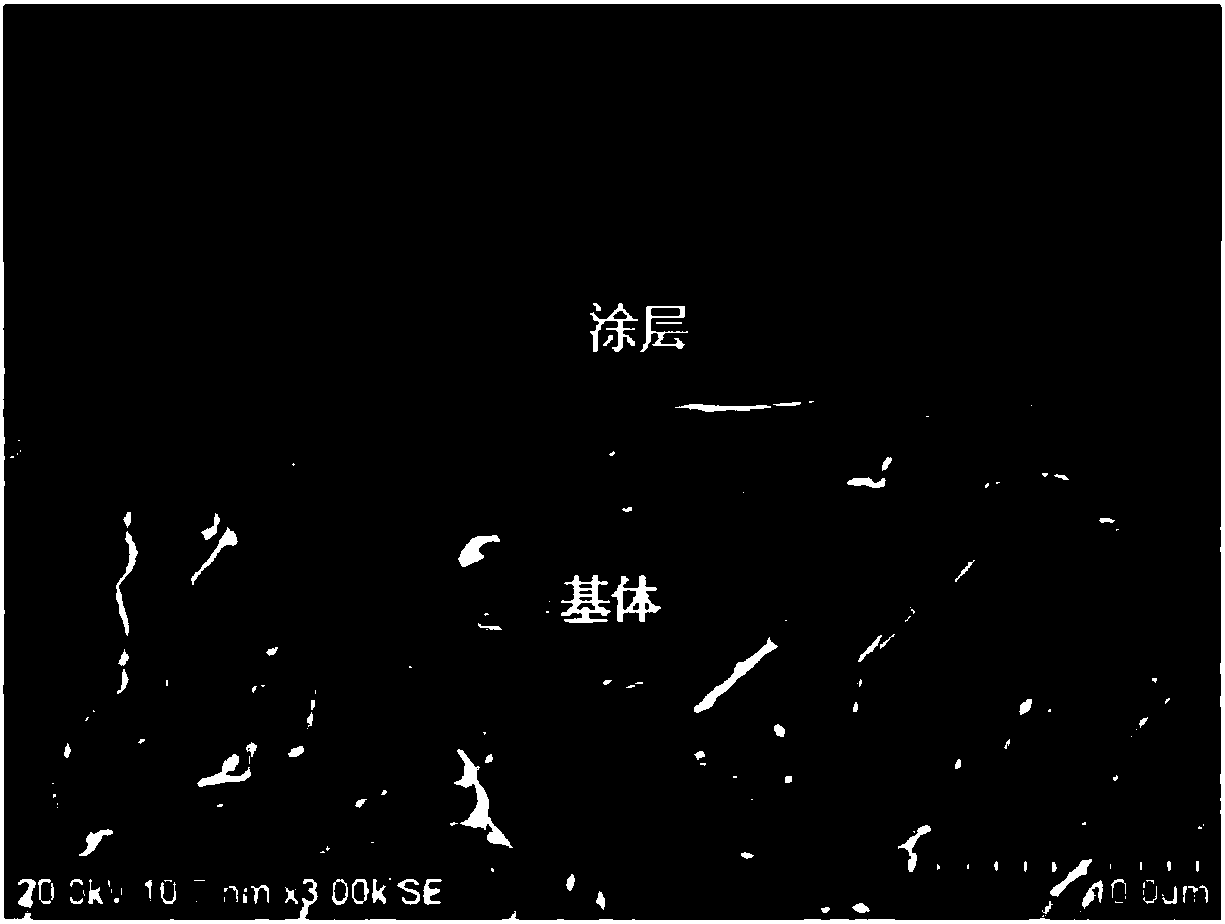
[0026] Plating transition layer: the substrate is made of stainless steel (grade 316L), the size of the sample is 20mm×10mm×10mm, and the size of the coating surface is 20mm×10mm. The surface before coating is ground, polished, ultrasonically cleaned and dried, and then placed on the sample stage of the vacuum chamber until the vacuum degree in the vacuum chamber reaches 4×10 -3 At Pa, heat the vacuum chamber to 300°C, feed argon gas into the vacuum chamber, set the gas flow rate to 100 sccm, control the air pressure at 2.0 Pa, apply pulse negative bias voltage -700V to the substrate, and perform glow cleaning on the sample for 10 minutes; Then, adjust the flow rate of argon gas to adjust the pressure of the vacuum chamber to 0.5Pa. At the same time, turn on the pure titanium target arc source, and the arc flow is stable at 70A. Ti + Bombard for 5 minutes; adjust pulse negative bias to -300V, deposit Ti film for 3 minutes, the thickness of the transition layer formed by Ti fil...
Embodiment 2
[0029] The substrate is made of titanium alloy (grade Ti6Al4V), the size of the sample is 20mm×10mm×10mm, and the size of the coated surface is 20mm×10mm. The surface before coating is ground, polished, ultrasonically cleaned and dried, and then placed on the sample stage of the vacuum chamber until the vacuum degree in the vacuum chamber reaches 4×10 -3 At Pa, turn on the gas mass flow controller, pass argon to 1.0Pa, apply a pulsed negative bias to -600V on the substrate, and perform glow cleaning on the sample for 15 minutes; then, adjust the flow of argon to adjust the pressure of the vacuum chamber to 0.6Pa, turn on the titanium target arc source at the same time, the arc current is stable at 80A, and perform Ti on the sample + Ion bombardment for 5 minutes; adjust the pulse negative bias to -200V, deposit the Ti metal layer for 3 minutes, and the thickness of the transition layer formed by the Ti film is 0.2 microns; then, use a pure titanium target, stop the argon and f...
Embodiment 3
[0032] The substrate is made of stainless steel (grade 1Cr18Ni9Ti), the size of the sample is 20mm×10mm×10mm, and the size of the coated surface is 20mm×10mm. The surface before coating is ground, polished, ultrasonically cleaned and dried, and then placed on the sample stage of the vacuum chamber until the vacuum degree in the vacuum chamber reaches 3×10 -3 At Pa, pass argon gas to 1.0Pa, apply pulse negative bias to -700V on the substrate, and perform glow cleaning on the sample for 5 minutes; then, adjust the Ar gas flow rate to adjust the vacuum chamber pressure to 0.3Pa, and turn on the titanium target arc at the same time source, the arc current was stabilized at 80A, and the samples were subjected to Ti +Ion bombardment for 4 minutes, the thickness of the transition layer formed by the Ti film is 0.2 microns; then, using a pure titanium target, stop the argon gas and feed nitrogen gas, adjust the air pressure to 1.0Pa; adjust the substrate pulse negative bias to -300V, ...
PUM
| Property | Measurement | Unit |
|---|---|---|
| thickness | aaaaa | aaaaa |
| thickness | aaaaa | aaaaa |
| thickness | aaaaa | aaaaa |
Abstract
Description
Claims
Application Information
 - Generate Ideas
- Intellectual Property
- Life Sciences
- Materials
- Tech Scout
- Unparalleled Data Quality
- Higher Quality Content
- 60% Fewer Hallucinations
Browse by: Latest US Patents, China's latest patents, Technical Efficacy Thesaurus, Application Domain, Technology Topic, Popular Technical Reports.
© 2025 PatSnap. All rights reserved.Legal|Privacy policy|Modern Slavery Act Transparency Statement|Sitemap|About US| Contact US: help@patsnap.com


