Aluminum nitride ceramic substrate line etching method
A technology of aluminum nitride ceramics and substrates, which is used in the removal of conductive materials by chemical/electrolytic methods, printed circuits, lithography/patterns, etc. and other problems to achieve the effect of ensuring uniformity
- Summary
- Abstract
- Description
- Claims
- Application Information
AI Technical Summary
Problems solved by technology
Method used
Image

Examples
Embodiment 1
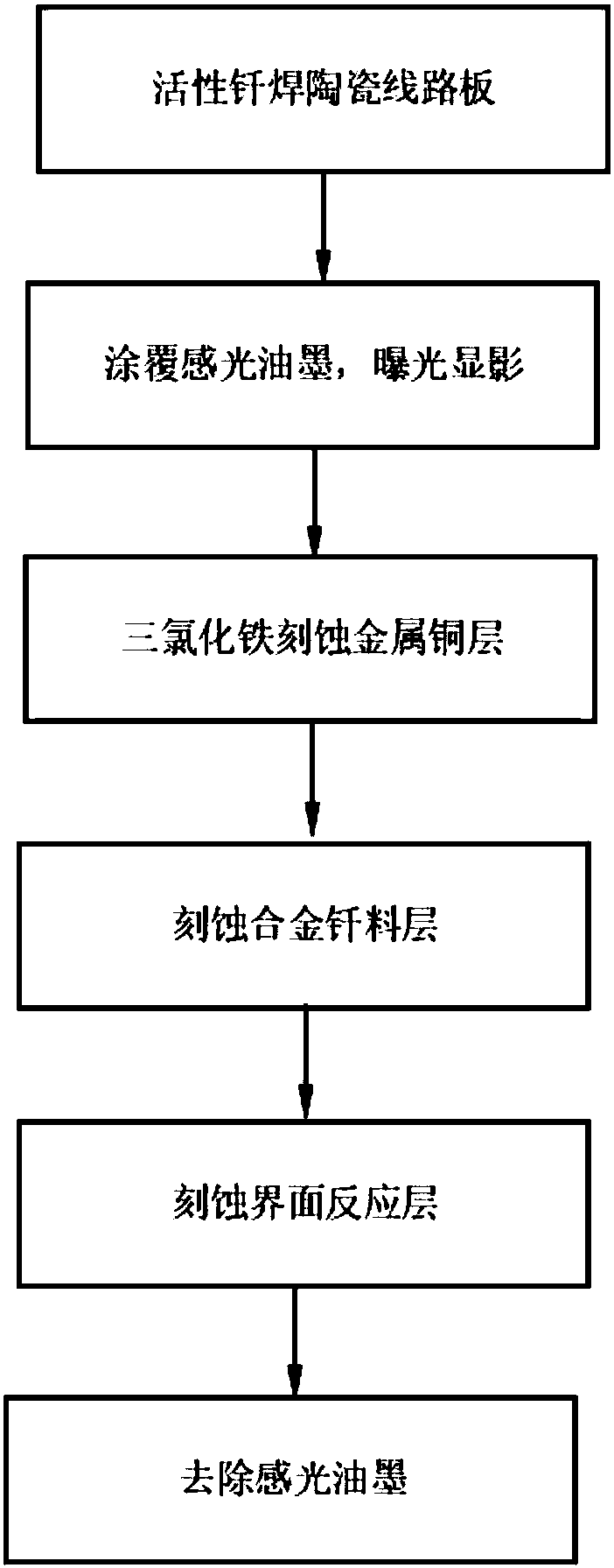
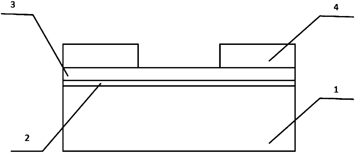
[0025] 1. The surface of the conductive metal copper layer of the aluminum nitride ceramic substrate is treated, coated with photosensitive ink, and the patterned photosensitive ink is cured on the metal side of the copper clad laminate after exposure and development, and the reaction of iron trichloride and copper is used to selectively remove Metal copper conductive layer 4 until the solder layer 3 is exposed, such as image 3 Shown.
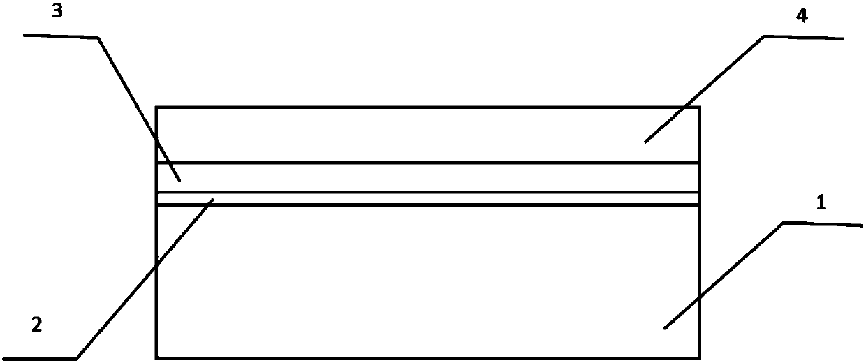
[0026] 2. At room temperature, immerse the sample exposed to the solder layer 3 into an etching solution of nitric acid and hydrogen peroxide with a volume ratio of 0.3:0.8 to react until the solder layer 3 is completely removed, until the interface reaction layer 2 is exposed, such as Figure 4 Shown.
[0027] 3. Immerse the sample exposing the interface reaction layer 2 into the etching solution of sulfuric acid hydrogen peroxide and water with a volume ratio of 0.5:0.3:0.1 until the interface reaction layer is completely removed and the ceramic s...
Embodiment 2
[0030] 1. The above steps are the same. At room temperature, immerse the sample exposed to the solder layer 3 into a 2:1.5 volume ratio of nitric acid and hydrogen peroxide etching solution to react until the solder layer 3 is completely removed, until the interface reaction layer is exposed 2. Such as Figure 4 Shown.
[0031] 2. Immerse the sample exposing the interface reaction layer 2 into the etching solution of sulfuric acid hydrogen peroxide and water with a volume ratio of 2:1.5:0.1 until the interface reaction layer is completely removed and the ceramic substrate is exposed, such as Figure 5 Shown.
Embodiment 3
[0033] 1. The above steps are the same. At room temperature, the sample exposed to the solder layer 3 is immersed in a 1:1 volume ratio of nitric acid and hydrogen peroxide etching solution to react until the solder layer 3 is completely removed, until the interface reaction is exposed Layer 2, such as Figure 4 Shown.
[0034] 2. Immerse the sample exposing the interface reaction layer 2 into the etching solution of sulfuric acid hydrogen peroxide and water with a volume ratio of 1:1:0.1 until the interface reaction layer is completely removed and the ceramic substrate is exposed, such as Figure 5 Shown.
[0035] In this embodiment, the temperature has little effect on the etching, and a large amount of heat is released during the reaction, and the reaction is preferably carried out at a normal temperature of 15-30°C.
[0036] In this embodiment, the aluminum nitride ceramic substrate is prepared using silver-copper-titanium active solder. After brazing, the alloy solder layer is ...
PUM
 Abstract
Description
Claims
Application Information
 - R&D
- Intellectual Property
- Life Sciences
- Materials
- Tech Scout
- Unparalleled Data Quality
- Higher Quality Content
- 60% Fewer Hallucinations
Browse by: Latest US Patents, China's latest patents, Technical Efficacy Thesaurus, Application Domain, Technology Topic, Popular Technical Reports.
© 2025 PatSnap. All rights reserved.Legal|Privacy policy|Modern Slavery Act Transparency Statement|Sitemap|About US| Contact US: help@patsnap.com