Solar-blind ultraviolet single-photon source and preparation method thereof
A single-photon source and sun-blind technology, applied to the structure of the active region and other directions, can solve the problem of no mature solution for single-photon sources
- Summary
- Abstract
- Description
- Claims
- Application Information
AI Technical Summary
Problems solved by technology
Method used
Image
Examples
Embodiment 1
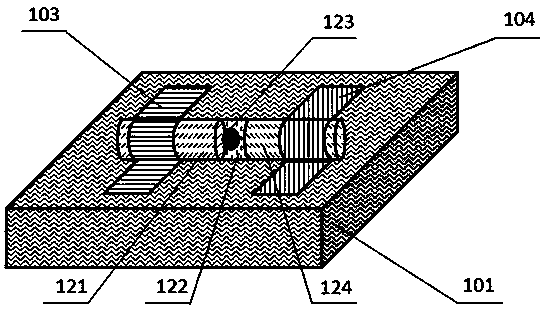
[0023] An AlGaN quantum dot embedded nanowire sun-blind single photon source lying flat on the substrate, as follows figure 1 As shown, among them: 103 is Si substrate; 121 is p-type Al 0.6 Ga 0.4 N nanowires, length 500 nm, diameter 40 nm; 122 is i-type Al 0.6 Ga 0.4 N layer, thickness 20 nm; 123 is Al 0.4 Ga 0.6 N single quantum dots, composed of quantum disks, the diameter of the disk is the same as that of nanowires, which is 40 nm, and the thickness of quantum disks is 0.5 nm; 124 is n-type Al 0.6 Ga 0.4 N nanowires with a length of 500 nm and a diameter of 40 nm; 103 is a p-type Au / Ti electrode; 104 is an n-type Au / Ni electrode. This single quantum dot embedded nanowire structure is firstly grown on a GaN substrate by MOCVD, then peeled off and laid flat on a Si substrate, and then electrodes are made at both ends of the nanowire. This AlGaN quantum dot embedded nanowire sun-blind single photon source has a luminous wavelength of 270 nm, and the luminous direction...
Embodiment 2
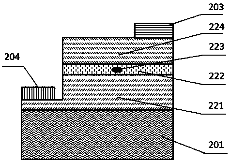
[0025] A sun-blind single photon source for InAlN quantum dots embedded in InAlGaN thin films, as follows figure 2As shown, where: 201 is AlN substrate; 221 is p-type In 0.1 al 0.7 Ga 0.2 N thin film with a thickness of 200 nm; 222 is i-type In 0.1 al 0.7 Ga 0.2 N film, thickness 10 nm; 223 is In 0.25 al 0.75 N quantum dots, grown by MBE self-assembly, the quantum dots are 2 nm in height, 10 nm in diameter, and have a density of 10 8 / cm 2 ; 24 is n-type In 0.1 al 0.7 Ga 0.2 N film with a thickness of 100 nm; 203 is a p-type graphene electrode; 204 is an n-type Au / Ni electrode. In this structure, the quantum dot embedded pin film is grown, and then the mesa is etched to expose the p-type layer, and then the p-type graphene electrode and the n-type Au / Ni electrode are prepared on the mesa. This sun-blind single photon source with InAlN quantum dots embedded in InAlGaN film emits at a wavelength of 256 nm. The preparation process does not require electron beam lith...
Embodiment 3
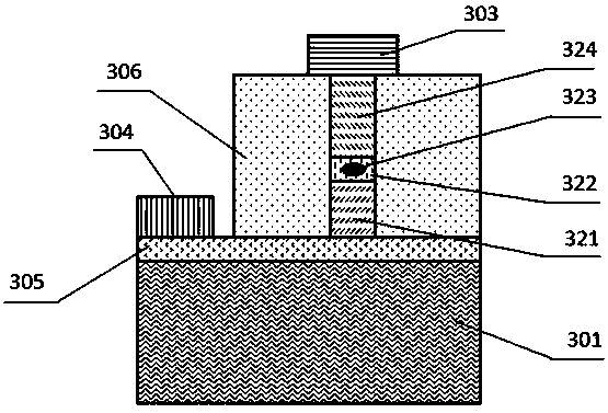
[0027] A ZnMgO quantum dot embedded nanowire sun-blind single photon source perpendicular to the substrate, as follows image 3 As shown, among them: 301 is MgO substrate; 321 is p-type Zn 0.6 Mg 0.4 O nanowires, length 300 nm, diameter 50 nm; 322 is i-type Zn 0.6 Mg 0.4 O nanowires, length 10 nm, diameter 50 nm; 323 is Zn 0.4 Mg 0.6 O quantum dots, the thickness is 2 atomic layers, the diameter is consistent with the nanowire, which is 50 nm; 324 is n-type Zn 0.6 Mg 0.4 O nanowire, length 100 nm, diameter 50 nm; 3 is p-type graphene electrode; 304 is n-type Au / Ni electrode; 305 is p-type Zn 0.6 Mg 0.4 O thin film; 306 is SOG. This structure was prepared by the Top-down method. Zn 0.6 Mg 0.4 O / Zn 0.4 Mg 0.6 O / Zn 0.6 Mg 0.4 O single quantum well is etched into a nanowire with a diameter of 50 nm to form a quantum dot embedded nanowire structure, and then the gap around the nanowire is filled with SOG, and then SOG is etched into a mesa to expose the underlying p-...
PUM
 Abstract
Description
Claims
Application Information
 - R&D Engineer
- R&D Manager
- IP Professional
- Industry Leading Data Capabilities
- Powerful AI technology
- Patent DNA Extraction
Browse by: Latest US Patents, China's latest patents, Technical Efficacy Thesaurus, Application Domain, Technology Topic, Popular Technical Reports.
© 2024 PatSnap. All rights reserved.Legal|Privacy policy|Modern Slavery Act Transparency Statement|Sitemap|About US| Contact US: help@patsnap.com


