


Quick Research
Generate reliable direction feasibility study reports for your R&D in just a few steps.

Technical Q&A
Discover and master advanced knowledge NOW. Basics, ideas, possibilities, all at once.

Find Solutions
As an expert in R&D theories, this can generate solutions to your technical problems instantly.

Evaluate Feasibility
Analyze your overall solution with one click, know your potential R&D risks in advance.

Monitor Landscape
Get weekly tech updates, stay abreast of the latest tech innovations and key insights.
A method of manufacturing a semiconductor device
A manufacturing method and semiconductor technology, applied in semiconductor/solid-state device manufacturing, electrical components, circuits, etc., can solve the problems of void exposure, uncontrolled STI step height, voids, etc., and achieve the effect of improving void problems.
- Summary
- Abstract
- Description
- Claims
- Application Information
AI Technical Summary
Problems solved by technology
Method used
Image

Examples
Embodiment 1
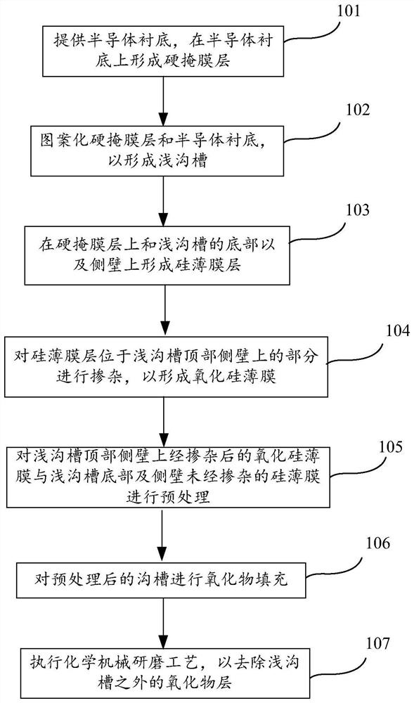
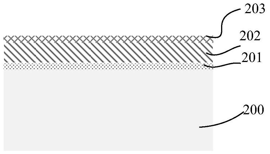
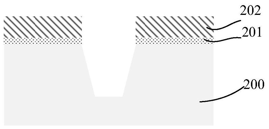
[0031] figure 1 A process flow diagram for making a semiconductor device according to an embodiment of the present invention; Figure 2A-2G A cross-sectional view of a structure formed in the relevant steps of making a semiconductor device according to an embodiment of the present invention; it will be combined below figure 1 and Figure 2A-2G The manufacturing method of the present invention will be described in detail.
[0032] Step 101 is executed to provide a semiconductor substrate on which a hard mask layer is formed.
[0033] Such as Figure 2A As shown in FIG. 1 , a structural cross-sectional view of a semiconductor substrate 200 and a hard mask layer sequentially formed on the semiconductor substrate 200 is shown in one embodiment of the present invention. The semiconductor substrate 200 may be at least one of the materials mentioned below: silicon, silicon-on-insulator (SOI), silicon-on-insulator (SSOI), silicon-germanium-on-insulator (S-SiGeOI), and germanium-on...
Embodiment 2
[0052] image 3 It is a process flow diagram of manufacturing a semiconductor device according to an embodiment of the present invention; Figures 4A-4H A cross-sectional view of the structure formed in the relevant steps of the manufacturing method for making a semiconductor device according to an embodiment of the present invention; image 3 and Figures 4A-4H The manufacturing method of the present invention will be described in detail.
[0053] Step 301 is executed to provide a semiconductor substrate on which a hard mask layer is formed.
[0054] Such as Figure 4A As shown, a cross-sectional view of the structure of the semiconductor substrate 400 and the hard mask layer sequentially formed on the semiconductor substrate 400 in one embodiment of the present invention is shown. The semiconductor substrate 400 may be at least one of the materials mentioned below: silicon, silicon-on-insulator (SOI), silicon-on-insulator (SSOI), silicon-germanium-on-insulator (S-SiGeOI)...
PUM
| Property | Measurement | Unit |
|---|---|---|
| thickness | aaaaa | aaaaa |
| thickness | aaaaa | aaaaa |
| thickness | aaaaa | aaaaa |
Abstract
Description
Claims
Application Information
 - R&D Engineer
- R&D Manager
- IP Professional
- Industry Leading Data Capabilities
- Powerful AI technology
- Patent DNA Extraction
Browse by: Latest US Patents, China's latest patents, Technical Efficacy Thesaurus, Application Domain, Technology Topic, Popular Technical Reports.
© 2024 PatSnap. All rights reserved.Legal|Privacy policy|Modern Slavery Act Transparency Statement|Sitemap|About US| Contact US: help@patsnap.com