Novel avalanche-diode photoelectric detector and preparation method thereof
An avalanche diode, photodetector technology, applied in circuits, electrical components, semiconductor devices, etc., to achieve the effect of reducing potential barriers, improving absorption efficiency, and reducing production costs
- Summary
- Abstract
- Description
- Claims
- Application Information
AI Technical Summary
Problems solved by technology
Method used
Image

Examples
preparation example Construction
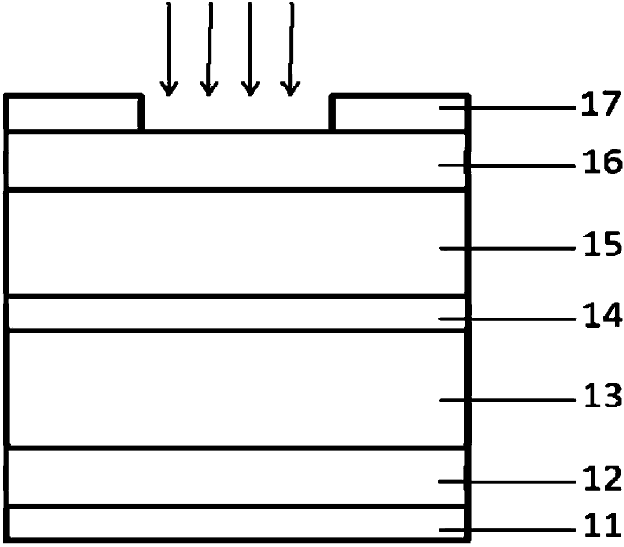
[0035] The preparation method of novel avalanche diode photodetector comprises the following steps:
[0036] 1) cleaning the single crystal substrate 13, removing the dirt particles and surface organic matter on the surface of the single crystal substrate 13, and drying it with a dryer;
[0037] 2) A metal multifunctional layer 14 with a thickness of 10-200 nm is epitaxially grown on the front surface of the single crystal substrate 13 by plasma enhanced chemical vapor deposition, molecular beam epitaxy or metal organic compound chemical vapor deposition, wherein the epitaxial growth temperature is 750-1150°C;
[0038] 3) An InGaAs absorbing layer 15 with a thickness of 1500-3000 nm is epitaxially grown on the metal multifunctional layer 14 by metal-organic compound chemical vapor deposition, wherein the epitaxial growth temperature is controlled at 900-1200° C.;
[0039] 4) epitaxially growing a P-type heavily doped InGaAs layer 16 with a thickness of 150-300 nm on the InGaA...
Embodiment 1
[0045] The preparation method of novel avalanche diode photodetector comprises the following steps:
[0046] 1) Clean the Si single crystal substrate with a standard cleaning process, remove the sticky particles and organic matter on the surface of the substrate, and dry it with a dryer;
[0047]2) Using MOCVD to epitaxially grow a layer of 20nm thick metal Al multifunctional layer on the front side of the Si single crystal substrate, the epitaxial growth temperature is 750°C;
[0048] 3) Using MOCVD to epitaxially grow a layer of 2000nm InGaAs absorption layer on the metal Al multifunctional layer, the growth temperature is controlled at 1050°C;
[0049] 4) Using MOCVD to epitaxially grow a layer of 300nm P-type heavily doped InGaAs on the InGaAs absorber layer, the growth temperature is controlled at 1050°C, and the doping element is Si;
[0050] 5) Use an ion implanter to uniformly implant ions on the back of the single crystal substrate, that is, the surface of the substr...
Embodiment 2
[0056] The preparation method of novel avalanche diode photodetector comprises the following steps:
[0057] 1) Clean the InP single crystal substrate with a standard cleaning process, remove the sticky particles and organic matter on the surface of the substrate, and dry it with a dryer;
[0058] 2) Using MOCVD to epitaxially grow a 20nm-thick metal Au multifunctional layer on the front side of the InP single crystal substrate, the epitaxial growth temperature is 750°C;
[0059] 3) Using MOCVD to epitaxially grow a layer of 2000nm InGaAs absorption layer on the metal Au multifunctional layer, the growth temperature is controlled at 1050°C;
[0060] 4) Using MOCVD to epitaxially grow a layer of 300nm P-type heavily doped InGaAs on the InGaAs absorber layer, the growth temperature is controlled at 1050°C, and the doping element is Si;
[0061] 5) Use an ion implanter to uniformly implant ions on the back of the single crystal substrate, that is, the surface of the substrate th...
PUM
| Property | Measurement | Unit |
|---|---|---|
| Thickness | aaaaa | aaaaa |
| Thickness | aaaaa | aaaaa |
| Thickness | aaaaa | aaaaa |
Abstract
Description
Claims
Application Information
 - R&D
- Intellectual Property
- Life Sciences
- Materials
- Tech Scout
- Unparalleled Data Quality
- Higher Quality Content
- 60% Fewer Hallucinations
Browse by: Latest US Patents, China's latest patents, Technical Efficacy Thesaurus, Application Domain, Technology Topic, Popular Technical Reports.
© 2025 PatSnap. All rights reserved.Legal|Privacy policy|Modern Slavery Act Transparency Statement|Sitemap|About US| Contact US: help@patsnap.com