
Compressively strained si CMOS device based on channel orientation selection and its fabrication method

A technology of crystal orientation selection and compressive strain, applied in semiconductor/solid-state device manufacturing, semiconductor devices, electric solid-state devices, etc., can solve the problem of poor hole mobility enhancement effect, etc. The effect of enhanced mobility and improved performance

Active Publication Date: 2020-06-05
XIDIAN UNIV
View PDF3 Cites 0 Cited by
  • Summary
  • Abstract
  • Description
  • Claims
  • Application Information

AI Technical Summary

Problems solved by technology

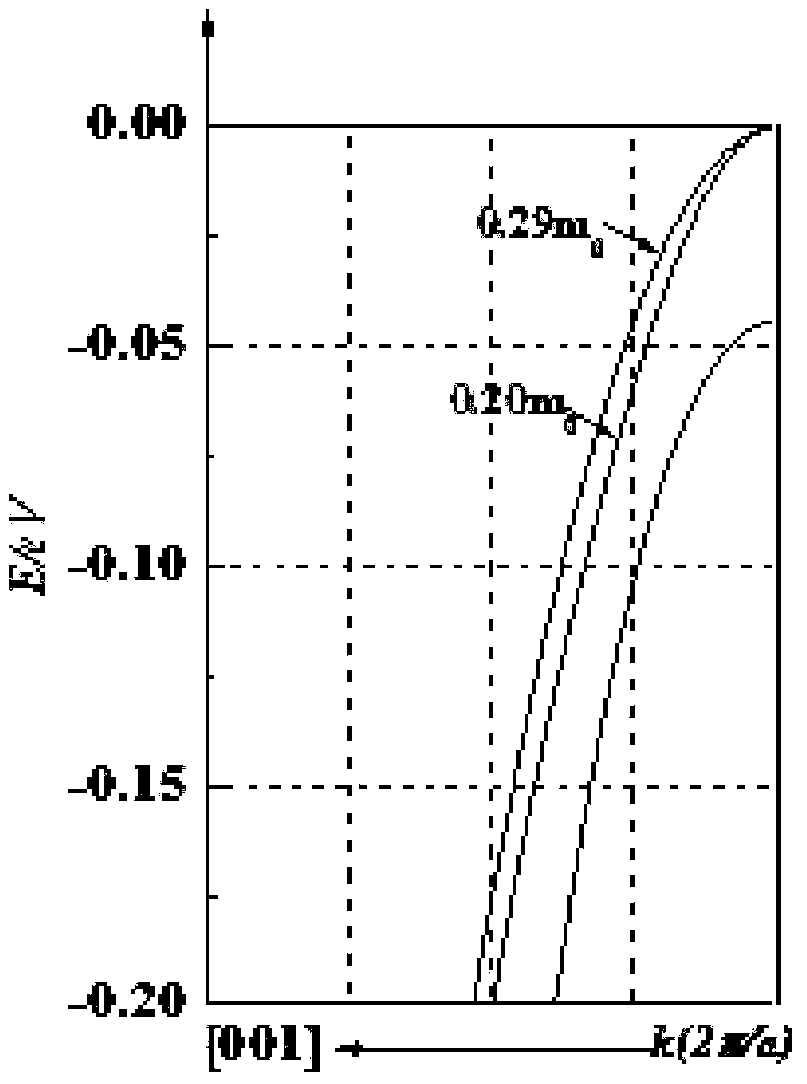
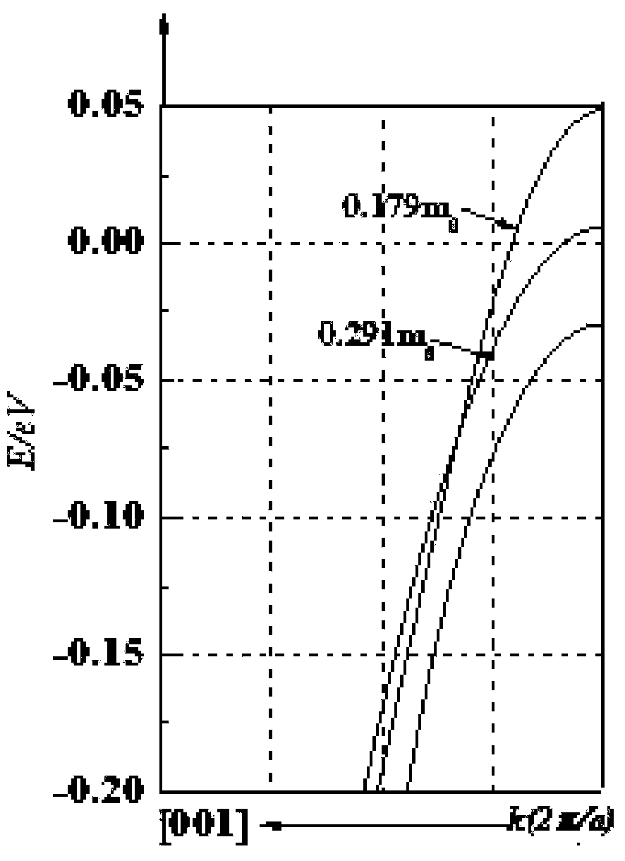
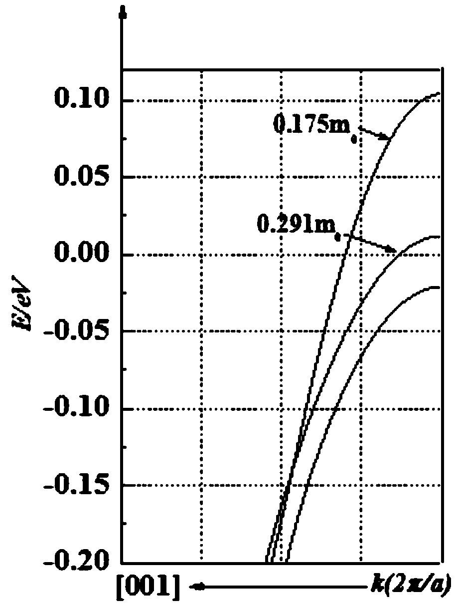
Although the overall hole mobility is improved under stress, the "offset" part leads to "poor" hole mobility enhancement effect

Method used


Image

  • Compressively strained si CMOS device based on channel orientation selection and its fabrication method
  • Compressively strained si CMOS device based on channel orientation selection and its fabrication method
  • Compressively strained si CMOS device based on channel orientation selection and its fabrication method

Examples


Embodiment 1

[0071] See figure 2 , figure 2 A process flow chart of a compressively strained Si CMOS device based on channel orientation selection provided by an embodiment of the present invention. The method comprises the steps of:

[0072] Step a, select Si substrate;

[0073] Step b, growing a relaxed SiC epitaxial layer on the surface of the Si substrate;

[0074] Step c, growing a strained Si layer on the surface of the relaxed SiC epitaxial layer;

[0075] Step d, forming shallow trench isolation in the strained Si layer, the relaxed SiC epitaxial layer and the Si substrate;

[0076] Step e, using an ion implantation process to form an N-type well region in a local area on the surface of the strained Si layer;

[0077] Step f, using an ion implantation process to form a P-type well region on the surface of the strained Si layer that is different from the N-type well region;

[0078] Step g, continuously growing a gate dielectric layer and a gate layer on the surface of the s...

Embodiment 2

[0103] See Figure 5a-Figure 5q , Figure 5a-Figure 5q A process schematic diagram of a compressively strained Si CMOS device based on channel orientation selection is provided for an embodiment of the present invention. On the basis of the above embodiments, this embodiment will introduce the process flow of the present invention in more detail. The method includes:

[0104] S101, substrate selection: such as Figure 5a As shown, a 2um thick doped silicon (Si) substrate 001 is selected as the initial material.

[0105] S102. Epitaxial layer growth:

[0106] S1021, such as Figure 5b As shown, a relaxed carbon-silicon epitaxial layer 002 with a thickness of 150-200 nm is grown by molecular beam epitaxy (MBE), and the carbon composition is about 1.30%-2%. The growth temperature is about 575-675°C, and the flow rate of the gas source is as follows: H 2 About 150ml / min, NPS about 50ml / min, SiCH 6 About 1ml / min;

[0107] S1022, such as Figure 5c As shown, a 10-20nm strai...

Embodiment 3

[0127]The present invention also provides a compressively strained Si CMOS device based on channel crystal direction selection, which includes: Si substrate layer, relaxed SiC epitaxial layer, strained Si layer, gate dielectric layer, metal gate layer, BPSG dielectric layer and W layer; wherein, the CMOS device is formed by the method described in the above-mentioned embodiment.


PUM

PropertyMeasurementUnit
thicknessaaaaaaaaaa
thicknessaaaaaaaaaa

Abstract

The invention relates to a compressive-strain Si CMOS device based on channel crystal orientation selection and a preparation method thereof. The preparation method comprises: selecting a Si substrate; growing a relaxed Si epitaxial layer; growing a strained Si layer; forming a shallow trench isolation; forming an N type well region and a P type well region by using an ion implantation process; growing a gate dielectric layer and a gate electrode continuously on the surface of the strained Si layer and etching the gate layer and the gate dielectric layer by using an etching process to form gates respectively; forming a PMOS source-drain region and an NMOS source-drain region based on a self-aligned process; and forming source-drain contact in the source-drain regions and then forming a CMOS device finally. Therefore, a problem of poor hole mobility enhancement effect of the biaxial strained Si material due to the traditional relaxed Si(1-x)Gex substrate is solved. The low-conductivity effective-quality [110] crystal orientation is used as biaxial strained Si / (001) Si(1- x)Cx PMOS channel orientation and the high-electron-mobility [100] crystal orientation as biaxial strained Si / (001) Si(1-x)CxNMOS channel orientation, so that the mobility ratio of the biaxial strained Si / (001) Si(1-x)Cx material and the performance of the device are improved.

Description

technical field [0001] The invention relates to the technical field of integrated circuits, in particular to a compressively strained SiCMOS device based on channel crystal direction selection and a preparation method thereof. Background technique [0002] Since the development of integrated circuits has slowed down as device feature sizes have entered the deep submicron range, physical issues have become more prominent. One is a series of problems caused by the enhancement of the internal electric field of the device, such as the reliability of the thin gate oxide layer, the influence of quantum effects, and the degradation of mobility; the other is that some parameters cannot be proportionally reduced with the size of the device, thus affecting the device and circuit. Performance impacts, such as the random fluctuations of impurities in the channel region, the influence of the source / drain region series resistance, and the design of the threshold voltage. These physical l...

Claims


Application Information

Patent Timeline
Patent Type & Authority Patents(China)
IPC IPC(8): H01L21/8238H01L27/092H01L29/04H01L29/16
CPCH01L21/823807H01L27/0928H01L29/045H01L29/16
Inventor 蒋道福宋建军苗渊浩胡辉勇宣荣喜张鹤鸣
Owner XIDIAN UNIV
Learn More