
Manufacturing method for high-speed PCB, and high-speed PCB

A production method and high-speed technology, applied in high-frequency matchers, printed circuit manufacturing, multi-layer circuit manufacturing, etc., can solve the problems of slow signal transmission rate, poor price and thermal stability, and achieve low conductor surface roughness, The effect of saving space and improving signal transmission quality

Inactive Publication Date: 2017-12-15
DONGGUAN SHENGYI ELECTRONICS
View PDF15 Cites 6 Cited by
  • Summary
  • Abstract
  • Description
  • Claims
  • Application Information

AI Technical Summary

Problems solved by technology

Especially for CCL material technology, the DK (dielectric constant) and Df (dissipation factor) of traditional FR-4 materials are relatively high, and high DK will slow down the signal transmission rate, and high Df will convert the signal part into heat energy loss In the substrate material, even if the circuit design is improved, the application requirements of high-speed signal transmission and signal integrity at high frequencies cannot be fully met. High-frequency materials with low DK and Df must be used to make copper clad substrates, but high-frequency materials Compared with FR-4 materials, the price is much higher and the thermal stability is relatively poor, so an effective solution is urgently needed

Method used


Image

  • Manufacturing method for high-speed PCB, and high-speed PCB
  • Manufacturing method for high-speed PCB, and high-speed PCB

Examples


Embodiment Construction

[0034] In order to make the purpose, features and advantages of the present invention more obvious and understandable, the technical solutions in the embodiments of the present invention will be clearly and completely described below in conjunction with the accompanying drawings in the embodiments of the present invention. Obviously, the following The described embodiments are only some, not all, embodiments of the present invention. Based on the embodiments of the present invention, all other embodiments obtained by persons of ordinary skill in the art without making creative efforts belong to the protection scope of the present invention.

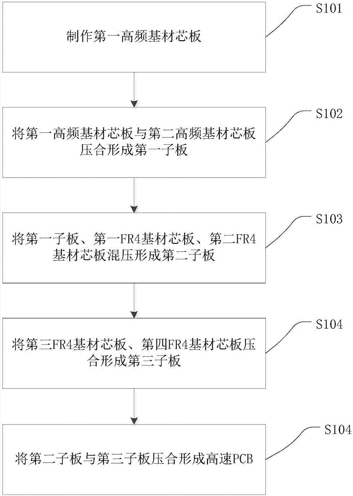
[0035] The core idea of ​​the present invention is: a new PCB product including stepped grooves, gold fingers and radio-frequency wires is produced by using multiple mixed pressing methods for high-frequency base material core boards and ordinary base material core boards. This PCB can realize the transmission of high-frequency microwave ...


PUM


Abstract

The invention discloses a manufacturing method for a high-speed PCB and the high-speed PCB, and the method comprises the steps: carrying out the stitching of at least two high-frequency base material core boards to form a first subboard; Carrying out the mixed pressing of the first subboard and at least one FR4 base material core board to form the high-speed PCB, wherein the outer core boards on two surfaces are respectively a high-frequency base material core board and an FR4 base material core board. The high-speed PCB is formed by the high-frequency base material core board and the FR4 base material core board in a mode of multiple mixed pressing, and the high-frequency base material core board serves as the outer core board. Because a high-frequency base material is low in dielectric constant and is low in loss factor, the transmission of high-frequency microwaves and other function signals can be achieved through manufacturing a radio frequency circuit on the first high-frequency base material core board, and the production cost is reduced at the same time. In addition, the second high-frequency base material core board is employed as the secondary outer core board, and a copper layer based on the second high-frequency base material core board is good in uniformity, thereby achieving the signal transmission through the combination of two sides, and greatly improving the signal transmission quality.

Description

technical field [0001] The present invention relates to the technical field of PCB (Printed Circuit Board, printed circuit board), in particular to a high-speed PCB manufacturing method and high-speed PCB. Background technique [0002] With the rapid development of information science and technology, various electronic consumer products with high-speed information processing functions have become an indispensable part of people's daily life, thus accelerating the transfer of wireless communication and broadband application industrial technology from the traditional military field to civilian consumption. The speed of transfer in the electronic field, due to the strong demand in the consumer electronics market, and constantly put forward higher technical requirements, such as high-speed information transmission, completeness, multi-functionality and miniaturization of products, etc., thus promoting the continuous development of high-frequency application technology . Especia...

Claims


Application Information

Patent Timeline
Patent Type & Authority Applications(China)
IPC IPC(8): H05K3/46H05K1/02H05K1/03
CPCH05K1/024H05K1/0298H05K1/036H05K3/4688H05K3/4697H05K2201/09845H05K2201/09981H05K2203/061
Inventor 王小平何思良纪成光袁继旺陈正清金侠
Owner DONGGUAN SHENGYI ELECTRONICS
Learn More