A kind of igbt silicon wafer back annealing method and laser annealing system
A technology of laser annealing and silicon wafers, which is applied in the direction of semiconductor devices, electrical components, circuits, etc., can solve the problems that silicon-based surface annealing cannot meet customer needs, etc.
- Summary
- Abstract
- Description
- Claims
- Application Information
AI Technical Summary
Problems solved by technology
Method used
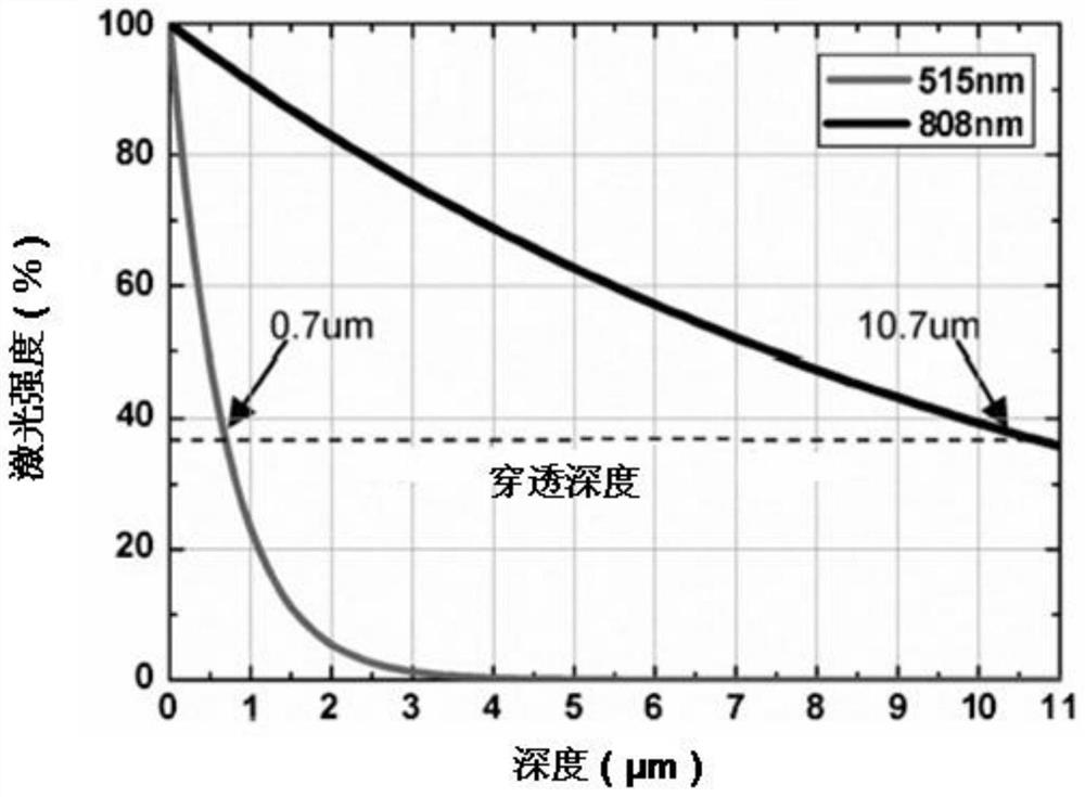
Image

Examples
Embodiment Construction
[0037] The specific embodiments of the present invention are given below in conjunction with the accompanying drawings, but the present invention is not limited to the following embodiments. Advantages and features of the present invention will be apparent from the following description and claims. It should be noted that all the drawings are in very simplified form and use imprecise ratios, which are only used for the purpose of conveniently and clearly assisting in describing the embodiments of the present invention.
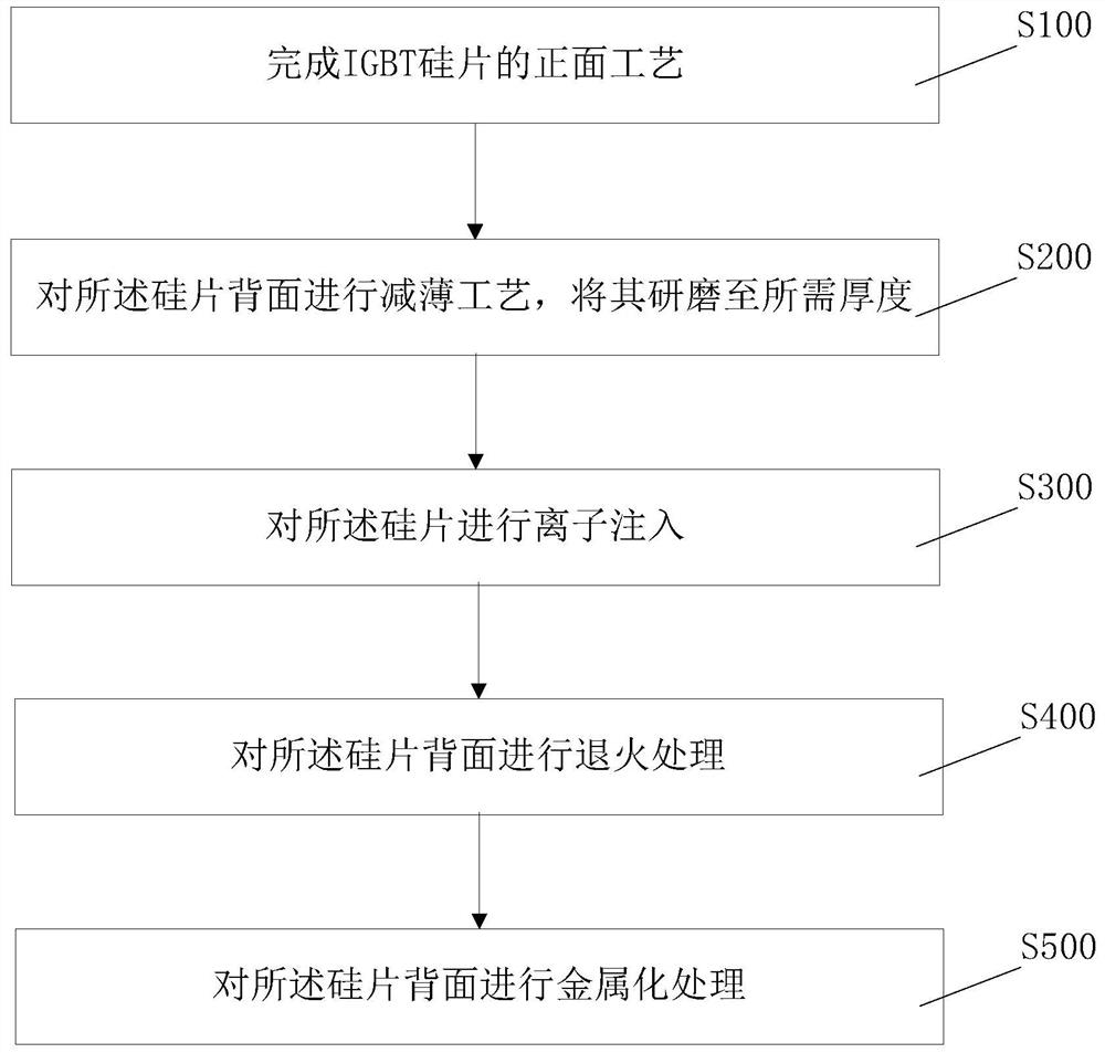
[0038] Please refer to figure 2 , figure 2 Shown is a flow chart of the back annealing method of the IGBT silicon wafer in a preferred embodiment of the present invention. The present invention proposes a kind of back annealing method of IGBT silicon chip, comprises the following steps:
[0039] Step S100: completing the front process of the IGBT silicon wafer;
[0040] Step S200: performing a thinning process on the back of the silicon wafer, and grindi...
PUM
 Abstract
Description
Claims
Application Information
 - R&D
- Intellectual Property
- Life Sciences
- Materials
- Tech Scout
- Unparalleled Data Quality
- Higher Quality Content
- 60% Fewer Hallucinations
Browse by: Latest US Patents, China's latest patents, Technical Efficacy Thesaurus, Application Domain, Technology Topic, Popular Technical Reports.
© 2025 PatSnap. All rights reserved.Legal|Privacy policy|Modern Slavery Act Transparency Statement|Sitemap|About US| Contact US: help@patsnap.com