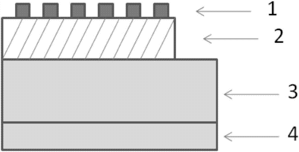
Resistance random access memory based on lead halide
A resistive memory, lead halide technology, applied in electrical components and other directions, can solve the problems of increasing power consumption and complexity of peripheral circuits, difficult to control the proportion of components, unclear application prospects, etc., to achieve high electrical stability, simple components, No effect of environmental pollution
- Summary
- Abstract
- Description
- Claims
- Application Information
AI Technical Summary
Problems solved by technology
Method used
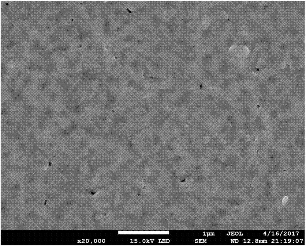
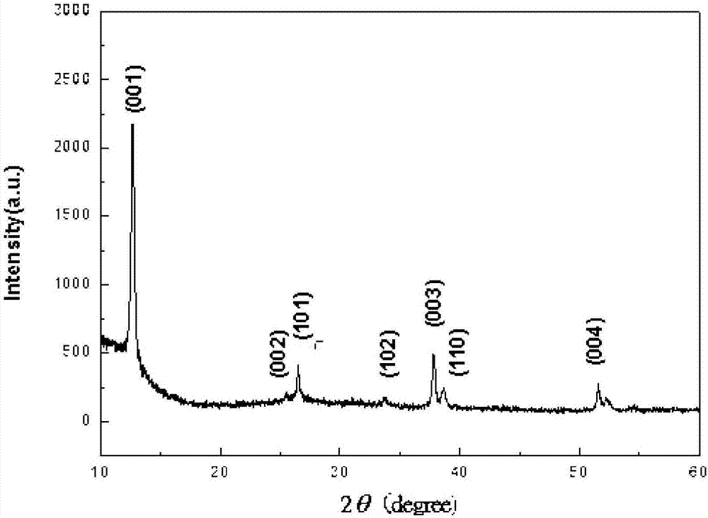
Image

Examples
Embodiment 1
[0037] Step 1. Clean the substrate
[0038] Wash the FTO with deionized water, acetone, and absolute ethanol in an ultrasonic instrument for 30 minutes respectively;
[0039] Step 2. Reserve electrodes
[0040] Paste a 4mm wide insulating tape on one side of the FTO conductive layer, and then irradiate the FTO surface with ultraviolet light for 30 minutes in a UV cleaner;
[0041] Step 3. Prepare lead iodide solution
[0042]Dissolve 0.462g of lead iodide powder in 1ml of dimethylformamide, place it in a thermostat at 70°C for 12 hours to completely dissolve the lead iodide powder in the solvent, and then filter it with a 0.45μm filter head;
[0043] Step 4. Spin coating and drying
[0044] The lead iodide solution was spin-coated onto the FTO surface with a spin coater at a speed of 3000 r / min for 30 seconds. Dry at 70°C for 30 minutes;
[0045] Step 5. Prepare the top electrode
[0046] The substrate in step 4 is placed in a magnetron sputtering device, and a top elect...
Embodiment 2
[0050] Step 1. Clean the substrate
[0051] Wash the FTO with deionized water, acetone, and absolute ethanol in an ultrasonic instrument for 30 minutes respectively;
[0052] Step 2. Reserve electrodes
[0053] Paste a 4mm wide insulating tape on one side of the FTO conductive layer, and then irradiate the FTO surface with ultraviolet light for 30 minutes in a UV cleaner;
[0054] Step 3. Prepare lead bromide solution
[0055] Dissolve 0.367g of lead bromide powder in 1ml of dimethyl sulfoxide, place it in a thermostat at 70°C for 12 hours to completely dissolve the lead bromide powder in the solvent, and then filter it with a 0.45μm filter head;
[0056] Step 4. Spin coating and drying
[0057] Spin coat the lead bromide solution onto the FTO surface with a spin coater at a speed of 3000 r / min for 30 seconds. Dry at 70°C for 30 minutes;
[0058] Step 5. Prepare the top electrode
[0059] The substrate in step 4 is placed in a magnetron sputtering device, and a top elect...
Embodiment 3
[0063] Step 1. Clean the substrate
[0064] Wash the FTO with deionized water, acetone, and absolute ethanol in an ultrasonic instrument for 30 minutes respectively;
[0065] Step 2. Reserve electrodes
[0066] Paste a 4mm wide insulating tape on one side of the FTO conductive layer, and then irradiate the FTO surface with ultraviolet light for 30 minutes in a UV cleaner;
[0067] Step 3. Prepare lead chloride solution
[0068] Dissolve 0.278g of lead chloride powder in 1ml of dimethyl sulfoxide, place it in a thermostat at 70°C for 12 hours to completely dissolve the lead chloride powder in the solvent, and then filter with a 0.45μm filter head;
[0069] Step 4. Spin coating and drying
[0070] The lead chloride solution was spin-coated on the FTO surface with a spin coater at a speed of 3000r / min for 30 seconds. Dry at 70°C for 30 minutes;
[0071] Step 5. Prepare the top electrode
[0072] The substrate was placed in the magnetron sputtering equipment, and a top elect...
PUM
 Abstract
Description
Claims
Application Information
 - R&D
- Intellectual Property
- Life Sciences
- Materials
- Tech Scout
- Unparalleled Data Quality
- Higher Quality Content
- 60% Fewer Hallucinations
Browse by: Latest US Patents, China's latest patents, Technical Efficacy Thesaurus, Application Domain, Technology Topic, Popular Technical Reports.
© 2025 PatSnap. All rights reserved.Legal|Privacy policy|Modern Slavery Act Transparency Statement|Sitemap|About US| Contact US: help@patsnap.com