Binary and multi-valued memristor based on HfO2-x, preparation method, and application of binary and multi-valued memristor

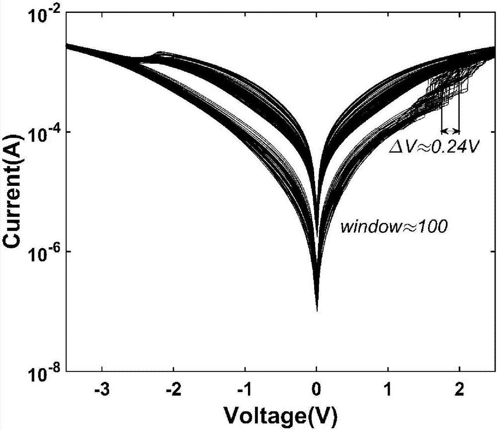
A 1.8 is unfavorable for memristor integration, unable to meet the demanding requirements of special-purpose chips, and functional decline.

Inactive Publication Date: 2017-10-24
HUAZHONG UNIV OF SCI & TECH
View PDF4 Cites 7 Cited by
  • Summary
  • Abstract
  • Description
  • Claims
  • Application Information

AI Technical Summary

Problems solved by technology

[0003] The above-mentioned implementation methods for memristors in different application fields have inevitable shortcomings
First of all, with the development of computing and storage fusion chips, different materials and processes are not conducive to the integration of different t...

Method used


Image

  • Binary and multi-valued memristor based on HfO2-x, preparation method, and application of binary and multi-valued memristor
  • Binary and multi-valued memristor based on HfO2-x, preparation method, and application of binary and multi-valued memristor
  • Binary and multi-valued memristor based on HfO2-x, preparation method, and application of binary and multi-valued memristor

Examples


Embodiment 1

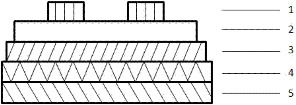
[0074] Example 1: Binary HfO 2-x Memristor

[0075] The binary HfO provided by embodiment 1 2-x Memristor, Pt / HfO with 8*8crossbar array structure x / Ti memristor, whose structure is as figure 1 shown; where the bottom electrode is Pt with a thickness of 100nm, and the functional layer is HfO with a thickness of 19.5nm 2-x , 2-x=1.93; the upper electrode is Ti with a thickness of 100nm.

[0076] The binary HfO of embodiment 1 is specifically described below 2-x The preparation method of memristor; Concrete steps are as follows:

[0077] (1) The first step: prepare the lower electrode:

[0078] (1.1) Photolithography: in the long SiO 2 One or more strip-shaped lower electrode patterns are prepared by a photolithography process on the Si substrate of the insulating layer;

[0079] Among them, the photolithography process includes: the steps of uniform glue, pre-baking, pre-exposure, post-baking, post-exposure, developing, coating, and stripping;

[0080] Sputtering: The...

Embodiment 2

[0094] Example 2: Multivalued HfO 2-x Memristor

[0095] The multi-valued HfO provided by embodiment 2 2-x Memristor, Pt / HfO with 8*8crossbar array structure x / Ti memristor, whose structure is as figure 1 shown; where the bottom electrode is Pt with a thickness of 100nm, and the functional layer is HfO with a thickness of 19.5nm 2-x , 2-x=1.69; the upper electrode is Ti with a thickness of 100nm.

[0096] The multi-valued HfO of embodiment 2 is specifically described below 2-x The preparation method of memristor; Concrete steps are as follows:

[0097] (1) The first step: preparing the lower electrode;

[0098] (1.1) Photolithography: in the long SiO 2 One or more strip-shaped lower electrode patterns are prepared by a photolithography process on the Si substrate of the insulating layer;

[0099] Among them, the photolithography process includes: the steps of uniform glue, pre-baking, pre-exposure, post-baking, post-exposure, developing, coating, and stripping;

[01...


PUM

PropertyMeasurementUnit
Thicknessaaaaaaaaaa
Thicknessaaaaaaaaaa
Thicknessaaaaaaaaaa

Abstract

The invention discloses a binary and multi-valued memristor based on HfO2-x, a preparation method, and an application of the binary and multi-valued memristor. The memristor comprises an upper electrode, a function layer, and a lower electrode. An HfO2-x material which has different grown-in oxygen vacant sites is prepared through the control of the proportion of argon to oxygen. In a DC scanning mode, an HfO2-x memristor with the low atomic ratio does not need to be preprocessed, is low in operation voltage and has the gradual-change resistance transition, but an HfO2-x memristor with the high atomic ratio is larger in window, and is sharper in resistance transition. Memristors in different resistance transition forms employ a continuous high-speed pulse and continuous multi-window pulse testing method to verify the binary and multi-valued mode. The resistance transition different represented by the memristor of the above type is of guide significance to the atomic ratio in different mode application occasions. The method can be used for logic calculation and neural morphology storage. The fine tuning of the proportion of deposition atmosphere is carried out under the same material technology, and the calculation and storage modules can be integrated in the same chip, thereby further speeding up the development of a calculation and storage integrated chip.

Description

technical field [0001] The invention belongs to the technical field of microelectronic devices, and more specifically, relates to an HfO-based 2-x Binary and multi-valued memristors, fabrication methods and applications thereof. Background technique [0002] Memristors in different application fields have different performance requirements. Logical computing pursues high speed and large windows, while neuromorphic computing requires multi-valued potential and low power consumption. These different applications put forward two challenges for memristors. value and multi-value requirements. At this stage, memristors for different application fields are mainly divided into two-value memristors with sharp resistance transition and multi-value memristors with gradual resistance transition through different materials and processes; A compromise option that meets the needs of most applications and implements general-purpose memristors; for some low-voltage application environments...

Claims


Application Information

Patent Timeline
IPC IPC(8): H01L45/00
CPCH10N70/883H10N70/011
Inventor 孙华军何维凡王标缪向水
Owner HUAZHONG UNIV OF SCI & TECH
Why Eureka
Try Eureka