Fabrication method of threshold voltage controllable gan-based enhanced device based on real-time monitoring of open gate structure parameters
A threshold voltage, real-time monitoring technology, applied in semiconductor/solid-state device manufacturing, electrical components, semiconductor devices, etc., can solve the problems of unable to manufacture HEMT devices, stay, unable to predict the threshold voltage range, etc., to achieve high operability and repeatability, repair damage, suppress negative drift
- Summary
- Abstract
- Description
- Claims
- Application Information
AI Technical Summary
Problems solved by technology
Method used
Image
Examples
Embodiment 1
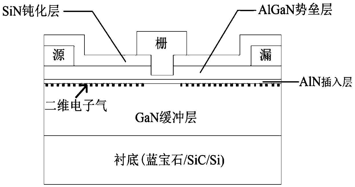
[0038] Embodiment 1, an AlGaN / GaN enhanced device with a threshold voltage of 0.2V is fabricated on a sapphire substrate.
[0039] Step 1: On the sapphire substrate, a GaN buffer layer, an AlN insertion layer, an AlGaN barrier layer and a GaN cap layer are sequentially grown from bottom to top by MOCVD process.
[0040](1a) Put the sapphire substrate into the MOCVD equipment, heat it up and keep it to 1050°C, then set the growth pressure of the chamber to 80Torr, the hydrogen flow rate to 5000 sccm, and the ammonia gas flow rate to 3000 sccm;
[0041] (1b) Introducing a gallium source with a flow rate of 200 sccm into the chamber, and growing a GaN buffer layer with a thickness of 650 nm on the sapphire substrate;
[0042] An aluminum source with a flow rate of 20 sccm is passed into the chamber, and an AlN insertion layer with a thickness of 1.5 nm is grown on the GaN buffer layer;
[0043] A gallium source with a flow rate of 200 sccm and an aluminum source with a flow rate...
Embodiment 2
[0133] Embodiment 2, an AlGaN / GaN enhanced device with a threshold voltage of 0.5V is manufactured on a silicon carbide substrate.
[0134] Step 1: On the silicon carbide substrate, a GaN buffer layer, an AlN insertion layer, an AlGaN barrier layer, and a GaN cap layer are sequentially grown from bottom to top by using an MOCVD process.
[0135] (1.1) Put the silicon carbide substrate into the MOCVD equipment, heat it up and keep it at 1000°C, then set the growth pressure of the chamber to 50Torr, the hydrogen flow rate to 4000 sccm, and the ammonia gas flow rate to 2000 sccm;
[0136] (1.2) Introduce a gallium source with a flow rate of 200 sccm into the chamber, and grow a GaN buffer layer with a thickness of 600 nm on the silicon carbide substrate;
[0137] An aluminum source with a flow rate of 20 sccm is passed into the chamber, and an AlN insertion layer with a thickness of 1 nm is grown on the GaN buffer layer;
[0138] A gallium source with a flow rate of 200 sccm and...
Embodiment 3
[0177] Embodiment 3, an AlGaN / GaN enhanced device with a threshold voltage of 0.8V is manufactured on a silicon substrate.
[0178] In step A, on the silicon substrate, a GaN buffer layer, an AlN insertion layer, an AlGaN barrier layer and a GaN cap layer are sequentially grown from bottom to top by MOCVD process.
[0179] (A1) Put the silicon substrate into the MOCVD equipment, heat it up and keep it at 1100°C, then set the growth pressure of the chamber to 60Torr, the hydrogen flow rate to 6000 sccm, and the ammonia gas flow rate to 4000 sccm;
[0180] (A2) Introducing a gallium source with a flow rate of 200 sccm into the chamber, and growing a GaN buffer layer with a thickness of 800 nm on the silicon substrate;
[0181] An aluminum source with a flow rate of 20 sccm is passed into the chamber, and an AlN insertion layer with a thickness of 2 nm is grown on the GaN buffer layer;
[0182] A gallium source with a flow rate of 200 sccm and an aluminum source with a flow rate...
PUM
 Abstract
Description
Claims
Application Information
 - R&D
- Intellectual Property
- Life Sciences
- Materials
- Tech Scout
- Unparalleled Data Quality
- Higher Quality Content
- 60% Fewer Hallucinations
Browse by: Latest US Patents, China's latest patents, Technical Efficacy Thesaurus, Application Domain, Technology Topic, Popular Technical Reports.
© 2025 PatSnap. All rights reserved.Legal|Privacy policy|Modern Slavery Act Transparency Statement|Sitemap|About US| Contact US: help@patsnap.com


