
III nitride-based heterojunction phototransistor

A phototransistor and nitride-based technology, which is applied in the field of visible light and ultraviolet light detectors, can solve the problems that the crystal quality of the epitaxial layer cannot be guaranteed, the dark current of the heterojunction phototransistor is high, and the junction interface between the base region and the emitter region is offset, etc. problems, to achieve the effects of improving impurity compensation, increasing response rate, and reducing the probability of recombination

Active Publication Date: 2017-09-22
SUN YAT SEN UNIV
View PDF5 Cites 7 Cited by
  • Summary
  • Abstract
  • Description
  • Claims
  • Application Information

AI Technical Summary

Problems solved by technology

In 1998, Wei Yang (Honeywell Technology Center) and others in the United States first reported the GaN / AlGaN-based visible light-blind heterojunction in the paper High gain GaN / AlGaN heterojunciton phototransistor (Applied Physics Letters, Vol. 73, No. 7). Phototransistor ultraviolet photodetector, the device adopts back-incidence structure, photocurrent gain, but the dark current of heterojunction phototransistor with this structure is relatively high, mainly because the epitaxial layer first grows AlGaN, GaN with large bandgap width The base region and the collector region are grown on it, so that the crystal quality of the epitaxial layer cannot be guaranteed
In 2001, Robert Mouillet et al. from Osaka Gas Co., Ltd. in Japan published the article Photoresponse and defect levels of AlGaN / GaN heterobipolar phototransistor grown on low-temperature AlN interlayer (Jpn. J. Appl. Phys, Vol. 40, pp. L498-L501) A visible light-blind AlGaN / GaN heterojunction phototransistor with a 45-degree normal incidence structure was reported, and its gain decreased as the light intensity weakened. It was found through testing that the p-type base material defect is the primary factor affecting the device. The structure of the device can realize weak light detection, but the photoelectric gain is not high
Compared with the previously reported structure, this device avoids the problem of crystal quality degradation caused by placing the AlGaN layer with a wider bandgap in the lower layer of the epitaxial structure, but due to the memory of the p-type base acceptor doped impurity Mg atoms effect, resulting in impurity compensation for the n-type emitter region and offset of the junction interface between the base region and the emitter region, which affects the improvement of device performance

Method used


Image

  • III nitride-based heterojunction phototransistor
  • III nitride-based heterojunction phototransistor
  • III nitride-based heterojunction phototransistor

Examples


Embodiment 1

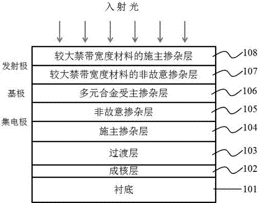
[0026] The structural schematic diagram of a kind of III-nitride-based heterojunction phototransistor of the present invention is as follows figure 1 As shown, it includes a substrate 101 and a Group-III nitride epitaxial layer grown on the substrate 101; wherein, the Group-III nitride epitaxial layer sequentially includes a nucleation layer 102, a transition layer 103, and a donor doped layer from bottom to top. 104 , an unintentional doped layer 105 , a multi-element alloy acceptor doped layer 106 , an unintentional doped layer 107 of a material with a larger band gap, and a donor doped layer 108 of a material with a larger band gap.

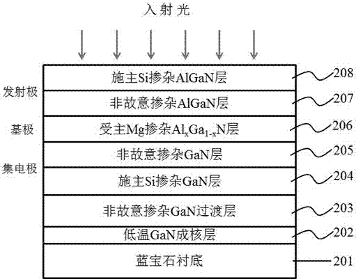
[0027] The following will combine figure 2 The structure of a group III nitride-based heterojunction visible light-blind ultraviolet (photoresponse cut-off wavelength ≤ 365 nm) phototransistor is specifically described. The structure of the ultraviolet phototransistor is npn type and adopts the form of normal incidence. Such as figure 2 As...

Embodiment 2

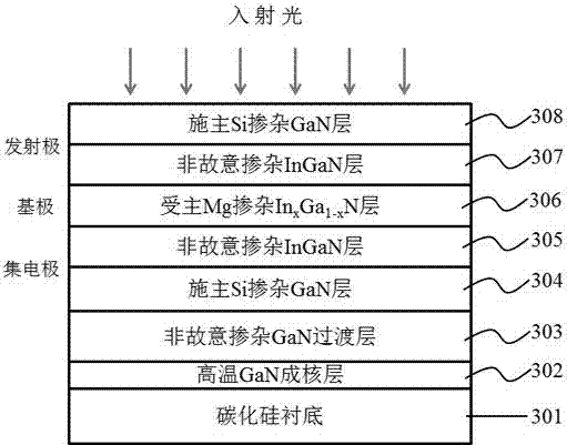
[0030] This implementation case 2 will specifically explain image 3 The structure of a group-III nitride-based heterojunction visible light (photoresponse cut-off wavelength ≤ 460 nm) phototransistor is shown. The structure of the visible light heterojunction phototransistor is npn type and adopts the form of normal incidence. Such as image 3 As shown, a III-nitride-based heterojunction phototransistor is grown by metal-organic chemical vapor deposition (MOCVD) or molecular beam epitaxy (MBE) epitaxial growth method, including a 6H-SiC substrate 301 and a III-nitride epitaxial layer 302 ~308, the Group-III nitride epitaxial layer includes a 25 nm thick high-temperature GaN nucleation layer 302 grown on a 6H-SiC substrate, an unintentionally doped GaN transition layer 303 with a thickness of 3.0 μm, and a transition layer 303 grown on the transition layer 303 1.0 μm thick donor Si heavily doped n-type GaN collector ohmic contact layer 304, 0.15 μm thick unintentionally doped...


PUM

PropertyMeasurementUnit
thicknessaaaaaaaaaa
thicknessaaaaaaaaaa
thicknessaaaaaaaaaa

Abstract

The invention relates to the technical field of visible light and ultraviolet light detectors and more particularly, relates to an III nitride-based heterojunction phototransistor. The III nitride-based heterojunction phototransistor comprises a substrate and an III nitride epitaxial layer growing on the substrate, wherein the III nitride epitaxial layer comprises a nucleating layer, a transition layer, a donor doping layer, an unintentionally doping layer, a multicomponent alloy acceptor doping layer, an unintentionally doping layer with a large band gap material, and a donor doping layer with a large band gap material sequentially from bottom to top. According to the III nitride-based heterojunction phototransistor, alloy components and the doping concentration graded base are adopted, an additional accelerated electric field is generated, transition of electrons through the base is accelerated, the possibility of being composited in the base is reduced, and the photoelectric gains and the detection sensitivity are further improved.

Description

technical field [0001] The present invention relates to the technical field of visible light and ultraviolet light detectors, and more specifically, relates to a group-III nitride-based heterojunction phototransistor that improves the transit efficiency of a carrier base region. Background technique [0002] Visible light and ultraviolet detection are widely used in various fields of military and national economy. Visible light detection has important applications in photometry, industrial automatic control, visible light imaging, visible light communication, etc.; It has the characteristics of less interference sources, and has important applications in fire alarm, environmental monitoring, high-voltage corona discharge detection, and industrial combustion process monitoring. In visible light and ultraviolet detection, visible light or ultraviolet photodetectors based on solid-state semiconductors have the advantages of small size, fast response speed, and high photoelectri...

Claims


Application Information

Patent Timeline
Patent Type & Authority Applications(China)
IPC IPC(8): H01L31/0304H01L31/11
CPCH01L31/03042H01L31/03044H01L31/03048H01L31/1105
Inventor 江灏张灵霞
Owner SUN YAT SEN UNIV
Learn More