Method for preparing submicron order crack-free ferrite film through step-by-step annealing technology
A ferrite thin film, sub-micron technology, applied in cathode sputtering applications, magnetic film to substrate applications, inductor/transformer/magnet manufacturing, etc., can solve problems such as cracking, reduce residual stress, and increase thickness. Effect
- Summary
- Abstract
- Description
- Claims
- Application Information
AI Technical Summary
Problems solved by technology
Method used
Image

Examples
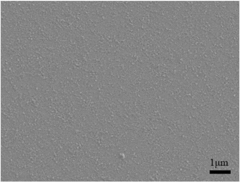
Embodiment 1
[0024] Step 1: Clean the surface of the substrate
[0025] Using single crystal silicon Si as the substrate, the thickness of the substrate is 500 μm, and the cleaning process is as follows:
[0026] (1) Ultrasonic cleaning with acetone for 10 to 12 minutes;
[0027] (2) Ultrasonic cleaning with absolute ethanol for 10 to 12 minutes;
[0028] (3) Ultrasonic cleaning with deionized water for 10 to 12 minutes;
[0029] (4) Dry the surface of the substrate with a nitrogen blow gun.
[0030] Step 2: Depositing thin films by RF magnetron sputtering
[0031] First the target (composition is Y 3 Fe 5 o 12 , target diameter is 70mm, thickness is 4mm) fixed on the target platform, and then the cleaned Si substrate is fixed on the abutment in the chamber, and the substrate is blocked by the baffle in the chamber, and the vacuum chamber is closed. Turn on the mechanical pump and the molecular pump in turn to draw vacuum until the background vacuum is lower than 3.0×10 -4 Pa. Tur...
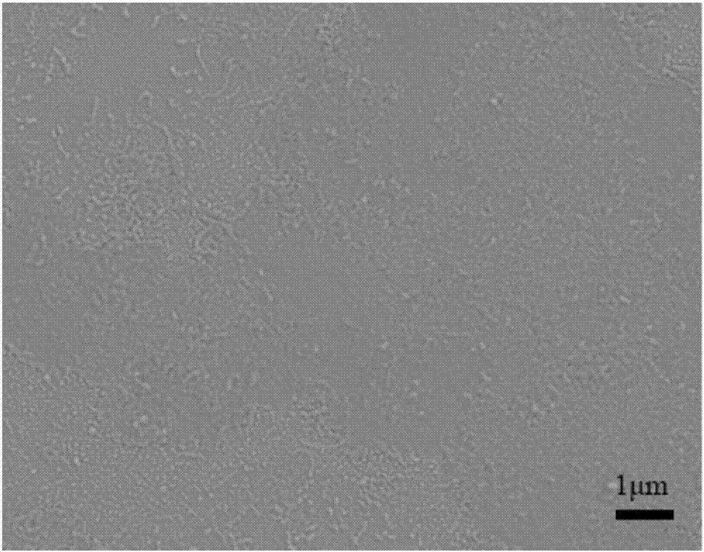
Embodiment 2
[0037] Step 1: Clean the surface of the substrate
[0038] Using single crystal silicon Si as the substrate, the thickness of the substrate is 500 μm, and the cleaning process is as follows:
[0039] (1) Ultrasonic cleaning with acetone for 10 to 12 minutes;
[0040] (2) Ultrasonic cleaning with absolute ethanol for 10 to 12 minutes;
[0041] (3) Ultrasonic cleaning with deionized water for 10 to 12 minutes;
[0042] (4) Dry the surface of the substrate with a nitrogen blow gun.
[0043] Step 2: Depositing thin films by RF magnetron sputtering
[0044] First the target (composition is Y 3 Fe 5 o 12 , target diameter is 70mm, thickness is 4mm) fixed on the target platform, and then the cleaned Si substrate is fixed on the abutment in the chamber, and the substrate is blocked by the baffle in the chamber, and the vacuum chamber is closed. Turn on the mechanical pump and the molecular pump in turn to draw vacuum until the background vacuum is lower than 3.0×10 -4 Pa. Tur...
PUM
| Property | Measurement | Unit |
|---|---|---|
| thickness | aaaaa | aaaaa |
| thickness | aaaaa | aaaaa |
| thickness | aaaaa | aaaaa |
Abstract
Description
Claims
Application Information
 - R&D
- Intellectual Property
- Life Sciences
- Materials
- Tech Scout
- Unparalleled Data Quality
- Higher Quality Content
- 60% Fewer Hallucinations
Browse by: Latest US Patents, China's latest patents, Technical Efficacy Thesaurus, Application Domain, Technology Topic, Popular Technical Reports.
© 2025 PatSnap. All rights reserved.Legal|Privacy policy|Modern Slavery Act Transparency Statement|Sitemap|About US| Contact US: help@patsnap.com