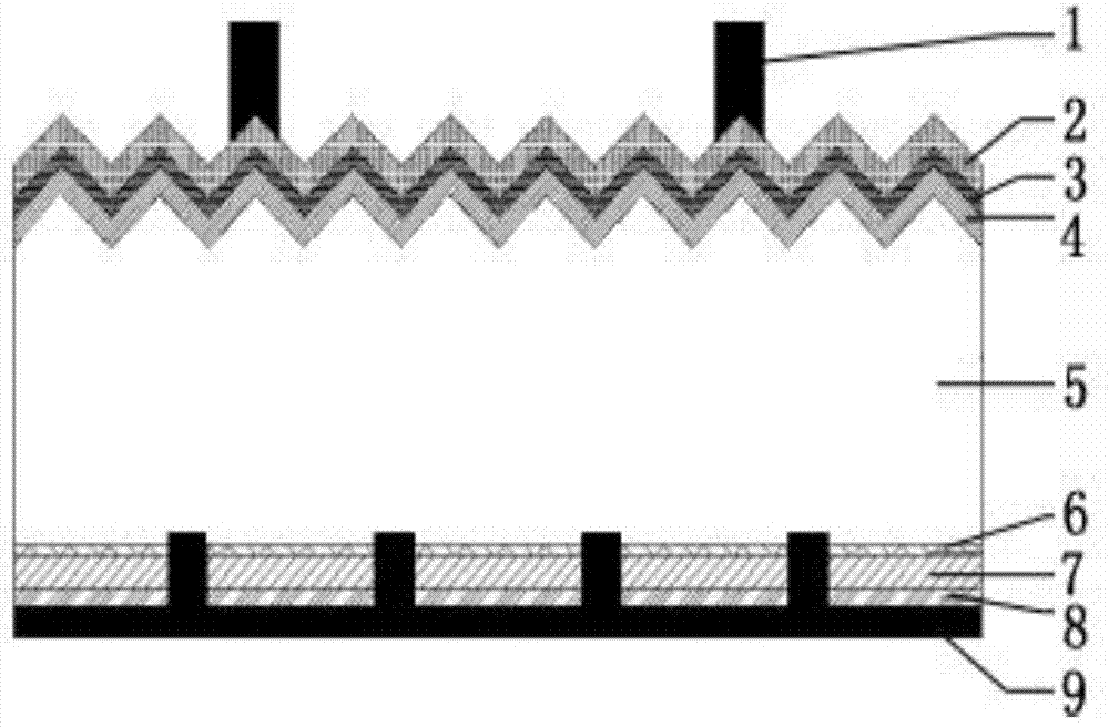
PERC cell back side passivation technology
A backside passivation and battery technology, which is applied in the field of solar cells, can solve the problems of poor matching between aluminum oxide and silicon of the backside passivation layer, poor surface passivation effect, and increased EL degradation, so as to improve field passivation. effect, increase the passivation effect, improve the effect of anti-PID performance
- Summary
- Abstract
- Description
- Claims
- Application Information
AI Technical Summary
Problems solved by technology
Method used
Image
Examples
Embodiment 1
[0033] A passivation process for the back of PERC cells, including texturing, diffusion, etching and back polishing, followed by hot air drying of silicon wafers, turning the silicon wafers 180° so that the back of the silicon wafers face up, and ozone treatment to form SiO on the back 2 film, the front side is oxidized, the back is plated with a passivation film, and the front side is plated with a passivation film; the front side is oxidized to be annealed to form SiO 2 membrane.
[0034]Specifically, 1. Texturing: use a chemical solution to etch the surface of the crystalline silicon wafer to form a suede surface with a light-trapping effect. The PN junction is formed on the silicon wafer at the bottom, and at present, the liquid source diffusion method of phosphorus oxychloride is mainly used.
[0035] 3. Etching and back polishing: acid bath (HF / HNO 3 / H 2 SO 4 ) etch to remove the edge PN junction and polish the backside - alkali bath (KOH) to neutralize the acid and...
Embodiment 2
[0044] A passivation process for the back of PERC cells, including texturing, diffusion, etching and back polishing, followed by hot air drying of silicon wafers, turning the silicon wafers 180° so that the back of the silicon wafers face up, and ozone treatment to form SiO on the back 2 film, the front side is oxidized, the back is plated with a passivation film, and the front side is plated with a passivation film; the front side is oxidized to be annealed to form SiO 2 membrane.
[0045] Specifically, 1. Texturing: use a chemical solution to etch the surface of the crystalline silicon wafer to form a surface textured surface with a light-trapping effect
[0046] 2. Diffusion: Put the crystalline silicon wafer into the diffusion furnace, and use the diffusion method to form a PN junction on the silicon wafer of the P-type substrate. At present, it is mainly the phosphorus oxychloride liquid source diffusion method.
[0047] 3. Etching and back polishing: acid bath (HF / HNO ...
Embodiment 3
[0056] A method for preparing a PERC cell, comprising: 1. Texturing: corroding the surface of a crystalline silicon wafer with a chemical solution to form a surface textured surface with a light-trapping effect
[0057] 2. Diffusion: Put the crystalline silicon wafer into the diffusion furnace, and use the diffusion method to form a PN junction on the silicon wafer of the P-type substrate. At present, it is mainly the phosphorus oxychloride liquid source diffusion method.
[0058] 3. Etching and back polishing: acid bath (HF / HNO 3 / H 2 SO 4 ) etch to remove the edge PN junction and polish the backside - alkali bath (KOH) to neutralize the acid and remove the porous silicon - acid bath (HF / HCL) to remove the front phosphosilicate glass, dry the silicon wafer with hot air, and turn the film with the turning machine. Ozone treatment on the back.
[0059] 4. Annealing treatment: Put the silicon wafer into the annealing furnace, pass a certain amount of oxygen during annealing, ...
PUM
| Property | Measurement | Unit |
|---|---|---|
| Thickness | aaaaa | aaaaa |
| Thickness | aaaaa | aaaaa |
| Thickness | aaaaa | aaaaa |
Abstract
Description
Claims
Application Information
 - R&D
- Intellectual Property
- Life Sciences
- Materials
- Tech Scout
- Unparalleled Data Quality
- Higher Quality Content
- 60% Fewer Hallucinations
Browse by: Latest US Patents, China's latest patents, Technical Efficacy Thesaurus, Application Domain, Technology Topic, Popular Technical Reports.
© 2025 PatSnap. All rights reserved.Legal|Privacy policy|Modern Slavery Act Transparency Statement|Sitemap|About US| Contact US: help@patsnap.com


