A kind of method for preparing SOI silicon chip with ultra-thick buried oxide layer

A technology of oxide layer and silicon wafer, which is applied in the manufacture of semiconductor/solid-state devices, electrical components, circuits, etc., can solve the problems of SOI wafer warping, poor film thickness uniformity, rough and not dense silicon dioxide layer surface, etc. Good strength, good density, and the effect of avoiding long-term high-temperature oxidation

Active Publication Date: 2020-11-06
SHENYANG SILICON TECH
View PDF4 Cites 0 Cited by
  • Summary
  • Abstract
  • Description
  • Claims
  • Application Information

AI Technical Summary

Problems solved by technology

Use the existing thermal oxidation process to prepare the silicon dioxide layer, the recommended thickness is 0.005μm-2μm, and some high-temperature, high-frequency, high-power, high-voltage optoelectronic and radiation-resistant devices and MEMC technical fields require an ultra-thick oxide layer As the SOI substrate of the isolation layer, this ultra-thick oxide layer refers to an oxide layer with a thickness of 2 μm-10 μm or more. The high temperature of the time will cause serious warping of the SOI wafer
The CVD process to prepare this ultra-thick buried oxide layer can avoid this phenomenon, but the surface roughness of the silicon dioxide layer grown by CVD chemical vapor deposition is not dense enough, and the film thickness uniformity is poor

Method used


Image

  • A kind of method for preparing SOI silicon chip with ultra-thick buried oxide layer
  • A kind of method for preparing SOI silicon chip with ultra-thick buried oxide layer
  • A kind of method for preparing SOI silicon chip with ultra-thick buried oxide layer

Examples


Embodiment 1

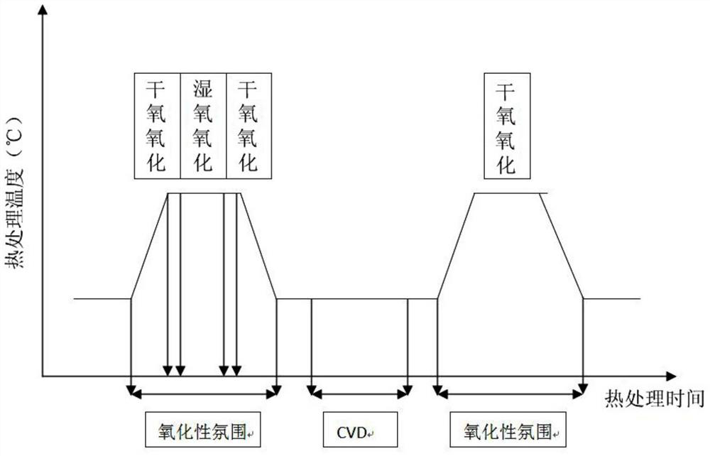
[0032] This embodiment is a method for preparing SOI silicon wafers with an ultra-thick buried oxide layer. Layer oxide layer SOI silicon chip; Wherein, the process flow of preparing buried layer oxide layer is as follows figure 1 As shown, the specific process is as follows:

[0033] 1) Loading the substrate monocrystalline silicon wafer into a sealed reaction chamber;

[0034] 2) The temperature of the reaction chamber is raised to 950°C-1100°C;

[0035] 3) Oxygen is fed into the reaction chamber (oxygen flow rate 5-10 liters / min), and the reaction time is 30-90 minutes to prepare a dense interface layer. The related reaction formula is: Si+O 2 → SiO 2 ;

[0036]4) The igniter is ignited, oxygen (oxygen flow rate 5-10 liters / min) and hydrogen (hydrogen flow rate 5-18 liters / min) are introduced into the reaction chamber, and the reaction time is 10-160 minutes to prepare a relatively dense interface layer. The related reaction formula for:

[0037] 2H 2 +O 2 →2H 2 o ...


PUM

PropertyMeasurementUnit
thicknessaaaaaaaaaa
thicknessaaaaaaaaaa
surface roughnessaaaaaaaaaa

Abstract

The invention discloses a method for preparing an SOI silicon chip with an ultra-thick buried oxide layer, wherein the method belongs to the field of semiconductor material preparation technology. According to the method of the invention, the SOI silicon chip with the ultra-thick buried oxide layer is prepared through successively performing buried oxide layer preparation, hydrogen ion injection, bonding and chip splicing on a monocrystalline silicon wafer, wherein the thickness of the buried oxide layer is 2-5 mu m. The preparation process of the buried oxide layer comprises a thermo-oxidizing process, a CVD process and a thermo-oxidizing process. The method of the invention can be used for preparing the ultra-thick buried oxide layer (with thickness of 2-5 mu m) and furthermore can obtain an SOI silicon chip bonding interface with relatively high surface compactness and relatively good interface state.

Description

technical field [0001] The invention relates to the technical field of semiconductor material preparation, in particular to a method for preparing an SOI silicon wafer with an ultra-thick buried oxide layer. Background technique [0002] SOI (Silicon-On-Insulator, silicon on insulating substrate) technology is to isolate the silicon dioxide film (buried layer oxide layer) between the top layer of silicon and the silicon substrate, so as to more effectively eliminate various body parasitic effects , greatly improving the performance of CMOS devices. Integrated circuits made of SOI materials also have the advantages of small parasitic capacitance, high integration density, fast speed, simple process, small short channel effect, and are especially suitable for low-voltage and low-power circuits. The mainstream technology of submicron low-voltage and low-power integrated circuits. [0003] An SOI wafer having a structure such as a base wafer, a buried oxide layer, and a device...

Claims


Application Information

Patent Timeline
Patent Type & Authority Patents(China)
IPC IPC(8): H01L21/762
CPCH01L21/76218
Inventor 范美华石文毛俭
Owner SHENYANG SILICON TECH
Why Eureka
Try Eureka