CdS-MoS2 nanoparticle co-doped black porous titanium dioxide photocatalyst
A nanoparticle, co-doping technology, applied in physical/chemical process catalysts, inorganic chemistry, hydrogen/syngas production, etc., can solve the problem of no reports on photocatalytic water splitting, and achieve the effect of high catalytic activity
- Summary
- Abstract
- Description
- Claims
- Application Information
AI Technical Summary
Problems solved by technology
Method used
Image
Examples
Embodiment 1
[0025] The molar ratio of embodiment 1 is 3%CdS-3%MoS 2 Nanoparticle co-doped black porous TiO 2 Synthesis of photocatalyst:
[0026] Add 1.5 mL of tetrabutyl titanate to a solution containing 1.5 mL of glacial acetic acid, 3 mL of deionized water and 10 mL of ethanol, and keep the above solution at 60°C for 12 hours to form a sol. Add 300mg of polystyrene balls, 35.2mg of cadmium acetate and 23.3mg of ammonium paramolybdate to the above sol-gel, and stir for 30min, then transfer to the reactor, and keep the temperature at 70°C for 12h to promote the formation of sol-gel again , and then the newly prepared sol-gel was calcined at 450°C for 6h under the condition of oxygen to obtain porous 3% MoO 3 -3%CdO-TiO 2 Intermediate product; 3% MoO will be prepared 3 -3%CdO-TiO 2 The intermediate product was added to an aqueous solution containing 300 mg of sodium borohydride and 30 mL of ethylenediamine, ultrasonicated for 30 minutes, then transferred to a reaction kettle, kept at...
Embodiment 2
[0028] Prepared according to the method described in Example 1 to obtain different MoS 2 -Black porous TiO with CdS doping 2 The results of photocatalyst and hydrogen production rate are shown in Table 1.
[0029] Table 1
Embodiment 3
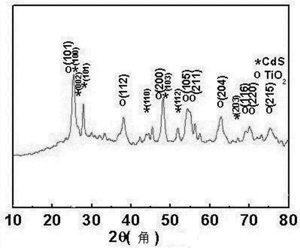
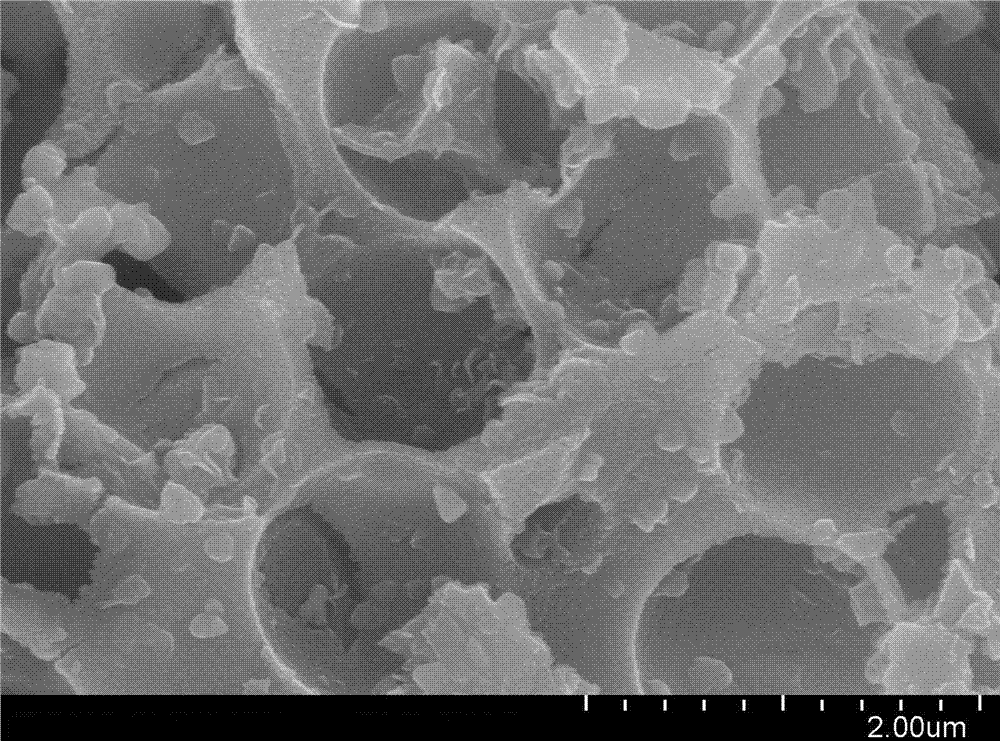
[0031] Example 3 MoS 2 -CdS nanoparticles co-doped black porous TiO 2 Characterization of photocatalyst complexes
[0032] (1) X-ray powder diffraction (XRD) characterization
[0033] The XRD test was carried out by a D8ADVANCE X-ray diffractometer produced by Germany Bruker Company. The test conditions are: the Kα radiation excited by the Cu target is the ray source, the Ni filter, the light source wavelength λ is 0.15406nm, the working voltage is 40kV, the current is 40mA, the scanning range is 20-80°, and the scanning speed is 4° / min .
[0034](2) Scanning electron microscope (SEM) characterization
[0035] It is mainly used to observe the microscopic morphology and particle size of the photocatalytic materials prepared in the experiment. The LEO1530VP field emission scanning electron microscope produced by Germany LEO Company was used for testing. Instrument parameters: resolution: 1nm (20kV); magnification: 20X-900,000X; acceleration voltage: 0.1-30kV. Due to the p...
PUM
 Abstract
Description
Claims
Application Information
 - R&D Engineer
- R&D Manager
- IP Professional
- Industry Leading Data Capabilities
- Powerful AI technology
- Patent DNA Extraction
Browse by: Latest US Patents, China's latest patents, Technical Efficacy Thesaurus, Application Domain, Technology Topic, Popular Technical Reports.
© 2024 PatSnap. All rights reserved.Legal|Privacy policy|Modern Slavery Act Transparency Statement|Sitemap|About US| Contact US: help@patsnap.com


